The core principles and value of HDI technology
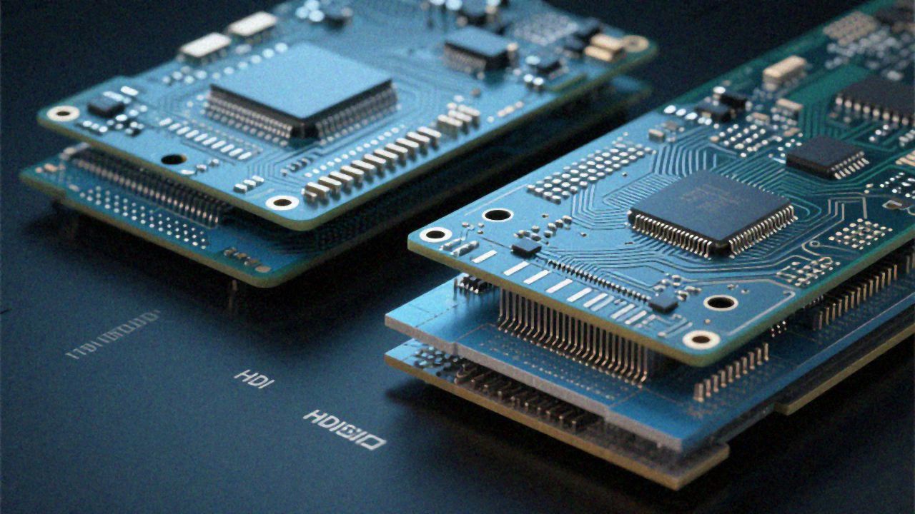
The core feature of HDI (High-Density Interconnect) is to accommodate more interconnection density in a smaller area through micro-blind hole and thin line technology. Compared with traditional through-hole PCBs, the routing density of HDI can be increased several times, and the signal integrity is also significantly improved. Prismark data shows that global PCB output value will reach US$85.152 billion in 2025, of which the proportion of HDI products continues to rise.
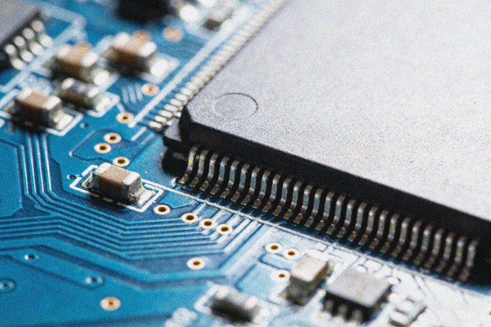
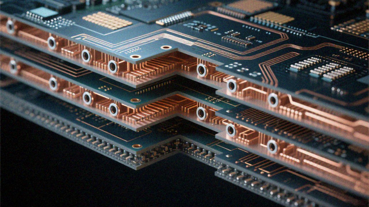
The interconnection of traditional through-hole PCBs relies on through-holes running through the entire board thickness. The diameter of the through-holes is usually more than 0.3 mm, occupying a large routing space. HDI technology introduces microvias, which can have a diameter of 0.1mm or less, and only connects two adjacent layers, without occupying the wiring space of other layers. This method of local interconnection significantly increases wiring density.
Thin wiring is another core feature of HDI. The line width and spacing of traditional PCBs are usually more than 4 mils, and HDI can be made 2 mils or even thinner. Thinning lines mean that more signal lines can be deployed per unit area, supporting more I/O interfaces and higher functional density.
The key role of HDI in the miniaturization of electronic products is reflected in three aspects. First, reduce the PCB area. Under the same functional requirements, the area of HDI PCB can be reduced by 30%-50% compared with traditional PCB. Second, improve signal integrity. The stub of the micro blind hole is shorter and has less impact on the reflection and impedance of high-speed signals. Third, support chips with higher pin density. The pin spacing of BGA packages continues to shrink, and HDI's fine wiring capabilities are the basis for high pin density chip routing.
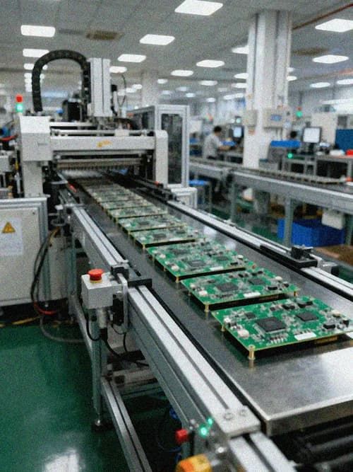
KINGBROTHER's HDI manufacturing capabilities cover 30 layers of arbitrary layer interconnects (sample)/26 layers of 4 levels (mass production), with a minimum line width and line spacing of 2.0/2.0mil (sample)/2.5/2.5mil (mass production), and a signal rate of up to 112Gbps (sample)/25Gbps (mass production). These process capabilities provide the technical foundation for HDI applications.
HDI process technical points
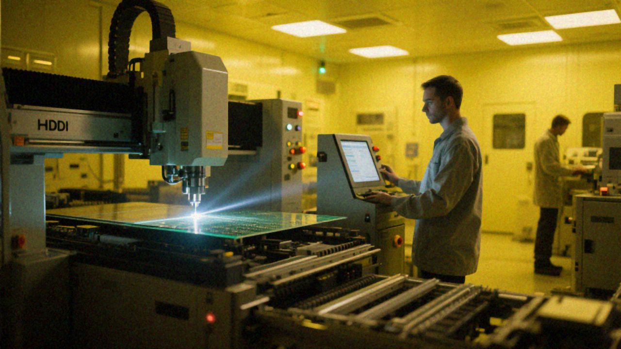
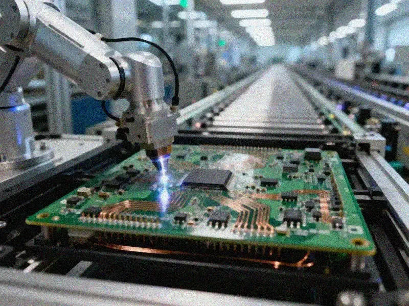
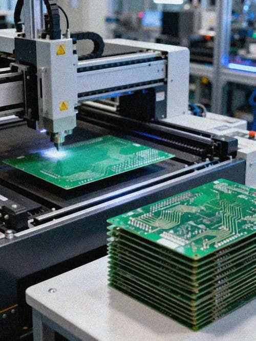
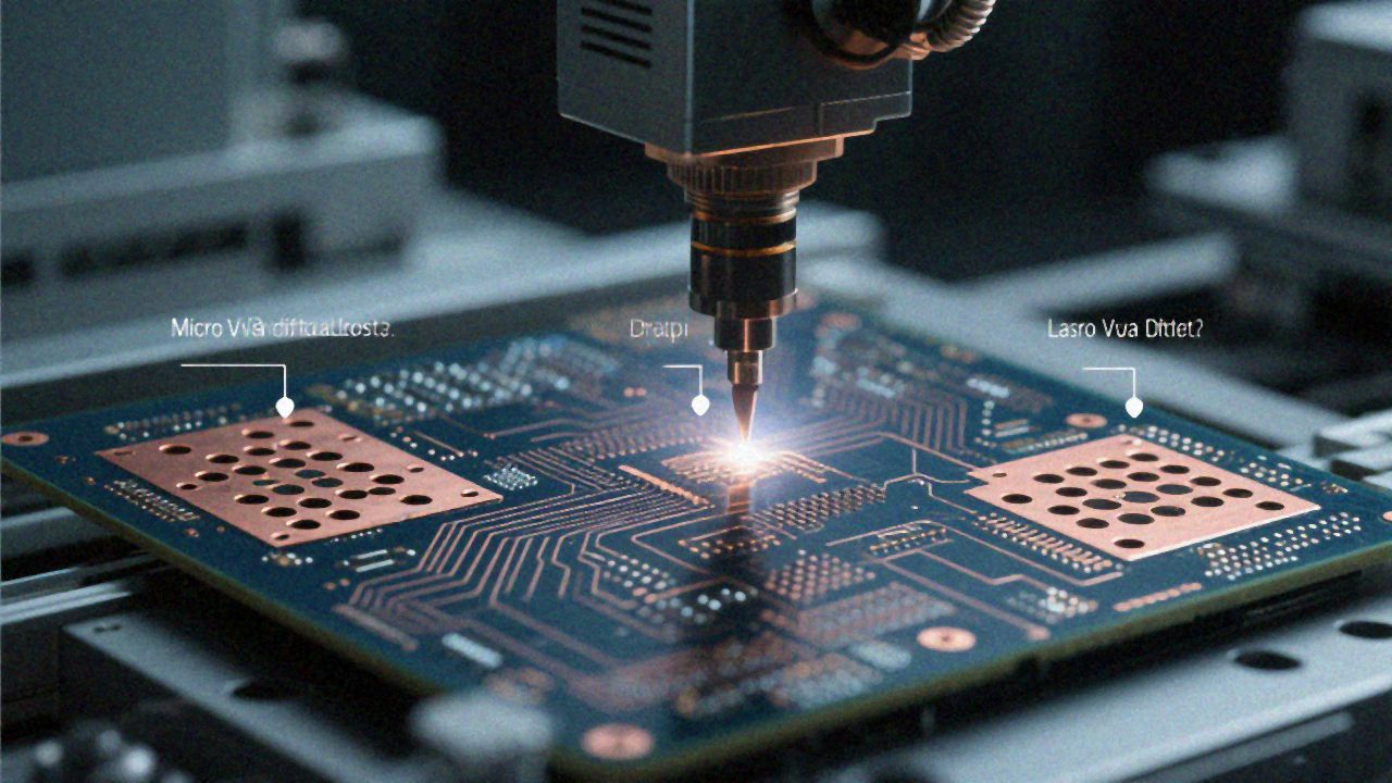
Micro-blind hole technology is the core process of HDI. Laser drilling is usually used to form micro-blind holes. Laser types include CO2 laser, UV laser, fiber laser, etc. Different laser types are suitable for different materials and application scenarios. CO2 laser is suitable for resin materials, UV laser is suitable for copper and resin, and fiber laser achieves a balance between accuracy and efficiency.
After laser drilling, micro-blind holes need to undergo hole metallization to form conductive paths. The process control of hole metallization directly affects the reliability of micro-blind holes. Hole wall roughness, copper plating thickness, and air bubbles in the hole are all process parameters that need to be controlled. KINGBROTHER's PCB manufacturing supports impedance control accuracy of ±5%(sample)/±10%(mass production), providing a process basis for impedance control of micro-blind holes.
Build-up is a typical method of HDI manufacturing. The lamination process deposits buildup layers layer by layer on the core, each layer containing micro blind holes and lines. Sequential Build-up is the most common method, one layer at a time to form micro blind holes layer by layer. Any-layer interconnection (Any-layer HDI) allows micro blind holes to be formed between any adjacent layers, making interconnection more flexible.
KINGBROTHER supports sample manufacturing of Any-layer HDI (HDI) with up to 30 layers. Compared with traditional order constraints such as 1+2+1, 2+2+2+2, arbitrary layer interconnections provide greater design freedom. For complex high-level HDI designs, arbitrary layer interconnections can optimize the routing topology and reduce the number of signal exchange levels.
Thin line technology is another technical point of HDI. The traditional subtractive process removes unwanted copper by etching to form a line. The subtractive method is limited by the etching factor, and it is difficult to make the line width and line spacing very thin. Semi-additive Process (SAP) and modified semi-additive process (mSAP) processes can achieve finer lines by depositing copper on a substrate and then selectively electroplating.
KINGBROTHER supports ENEPIG surface treatment and embedded chip technology, providing process support for high-end applications of HDI. ENEPIG (Electroless Nickel Electroless Palladium Immersion Gold) surface treatment has excellent welding performance and gold wire bonding performance, making it suitable for high-reliability applications. Embedded chip technology allows passive devices or bare chips to be embedded inside the PCB, further increasing functional density.
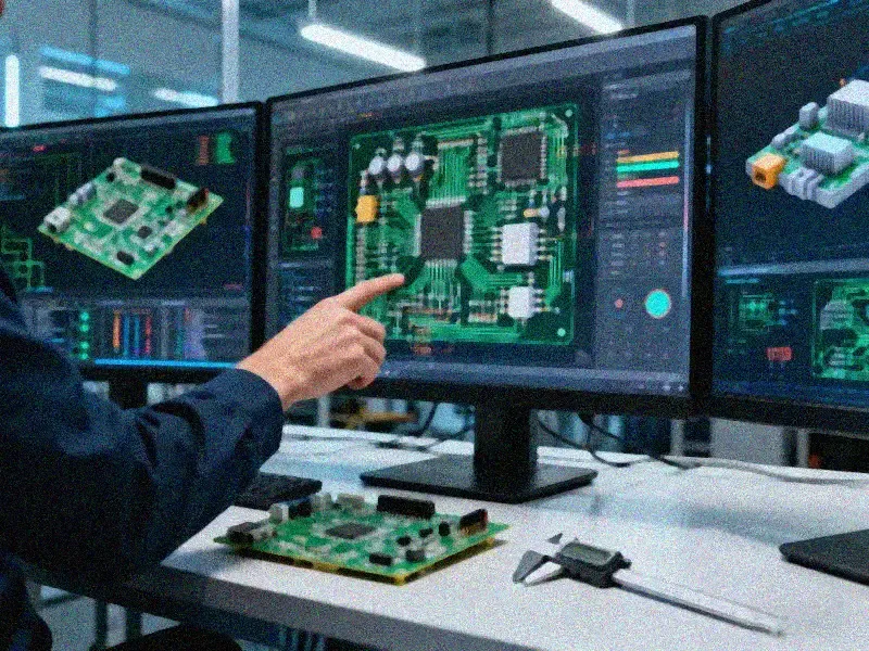
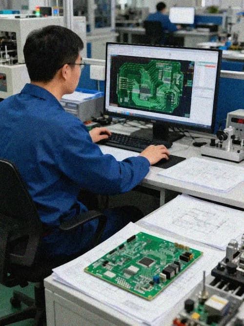
DFM (Design for Manufacturability) is an important consideration in HDI design. KINGBROTHER has established a database of 3.27 million certified materials and 2368 DFM rules, providing data support for HDI's manufacturability design. The design rules of HDI are more complex than traditional PCBs. The size, location, and stacking relationship of micro blind holes, as well as the width, spacing, and direction of the lines, all need to be optimized under manufacturability constraints.
Typical application scenarios of HDI
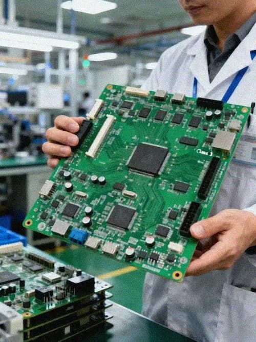
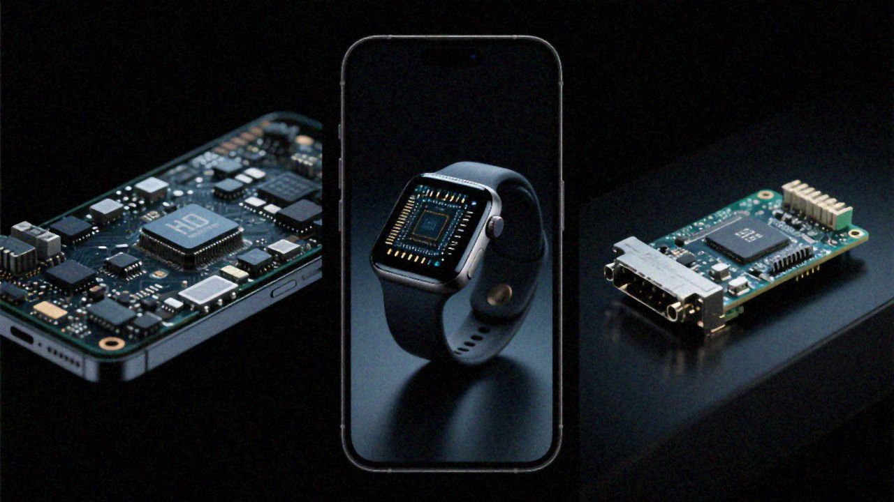
Smartphones are HDI's largest application market. The motherboard of smartphones requires the integration of many functional modules such as processors, memory, storage, communications, cameras, and sensors within a limited area, and the requirements for wiring density are extremely high. Typical smartphone motherboards use 6-10 layers of HDI design, and some high-end models use any layer of interconnection HDI.
HDI is also widely used in daughter boards and radio frequency modules of smartphones. Radio frequency modules have high requirements for signal integrity. HDI's micro blind vias can reduce signal layer swapping stubs and improve high-frequency performance. The connector board area of the camera module is limited, and the fine wiring capabilities of HDI are the basis for high-pixel camera interface wiring.
Wearable devices are an emerging application in HDI. Wearable devices such as smart watches, wireless headphones, and AR glasses have strict limits on the size and weight of PCBs. HDI can achieve sufficient functional density in a very small area and is the mainstream choice for wearable device PCBs.
Automotive electronics are a growth application for HDI. ADAS domain controllers, smart cockpits, vehicle communication modules, etc., have high requirements on the functional density and signal integrity of PCBs. Automotive electronics HDI needs to meet the IATF16949 quality system and IPC Class 3 reliability standards, and has strict requirements on manufacturing processes and quality control.
KINGBROTHER demonstrated a 16-layer HDI design with Rogers/M6 high-frequency material in its IPDM solution for the automotive industry. High-frequency materials have lower dielectric losses and are suitable for high-speed interfaces such as automotive Ethernet and SerDes. A 20-layer high-frequency board and shield design case in the medical industry demonstrates HDI's design experience in high-reliability applications.
High-speed communications is another important application for HDI. KINGBROTHER has the design and manufacturing capabilities of 56-layer 112Gbps high-speed PCB to support the high-speed interconnection needs of data centers and communication equipment. The design points of high-speed HDI include: impedance control, loss control, crosstalk control, and via optimization, each of which requires careful design and simulation verification.
Development Trend of HDI Technology
Any layer interconnection of HDI is an important direction of technology evolution. Traditional order constraints (such as 1+2+1, 2+2+2) restrict the degree of design freedom. Any layer interconnection breaks this constraint and allows micro-blind holes to be formed between any adjacent layers. The fabrication of arbitrary layer interconnects is more difficult and requires finer alignment control and more stable process parameters.
KINGBROTHER supports the sample manufacturing of 30-layer arbitrary layer interconnected HDI, providing a technical foundation for high-end applications. The design of arbitrary layer interconnection HDI needs to consider factors such as density limitations of micro-blind vias, thermal stress distribution, and reliability verification, and the design complexity is significantly higher than that of traditional HDI.
mSAP process is the evolution direction of thin circuit technology. mSAP can achieve 1mil or even thinner lines, further improving wiring density. The mSAP process has high equipment investment and process control requirements, and is currently mainly used in high-end applications. As the process matures and costs decrease, the application scope of mSAP will gradually expand.
Integration with IC carrier boards is a long-term trend in HDI. The package Substrate is the substrate for chip packaging, with thinner lines, more layers of layers, and more complex processes. The technical boundary between HDI and IC carrier boards is blurring, and some high-end HDI processes are close to IC carrier boards. This convergence trend places higher requirements on the process capabilities of PCB suppliers.
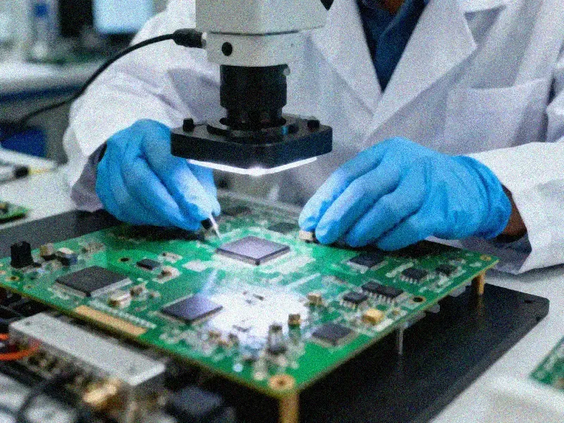
KINGBROTHER's PCB manufacturing capabilities cover up to 72 layers (sample)/32 layers (mass production) of FR4. In conjunction with the testing capabilities of an ISO/IEC17025 certified laboratory, it provides a test basis for reliability verification of HDI. The EMC test pass rate reached 98.5%, providing data support for the electromagnetic compatibility design of HDI.
The evolution direction of HDI technology is moving towards thinner lines and more flexible interconnection structures. The maturity of arbitrary layer interconnections and mSAP processes will further reduce the proportion of physical space of PCBs in electronic products. For teams planning the architecture of next-generation electronic products, it is a reasonable rhythm arrangement to evaluate the process capabilities and mass production experience of HDI suppliers in advance.