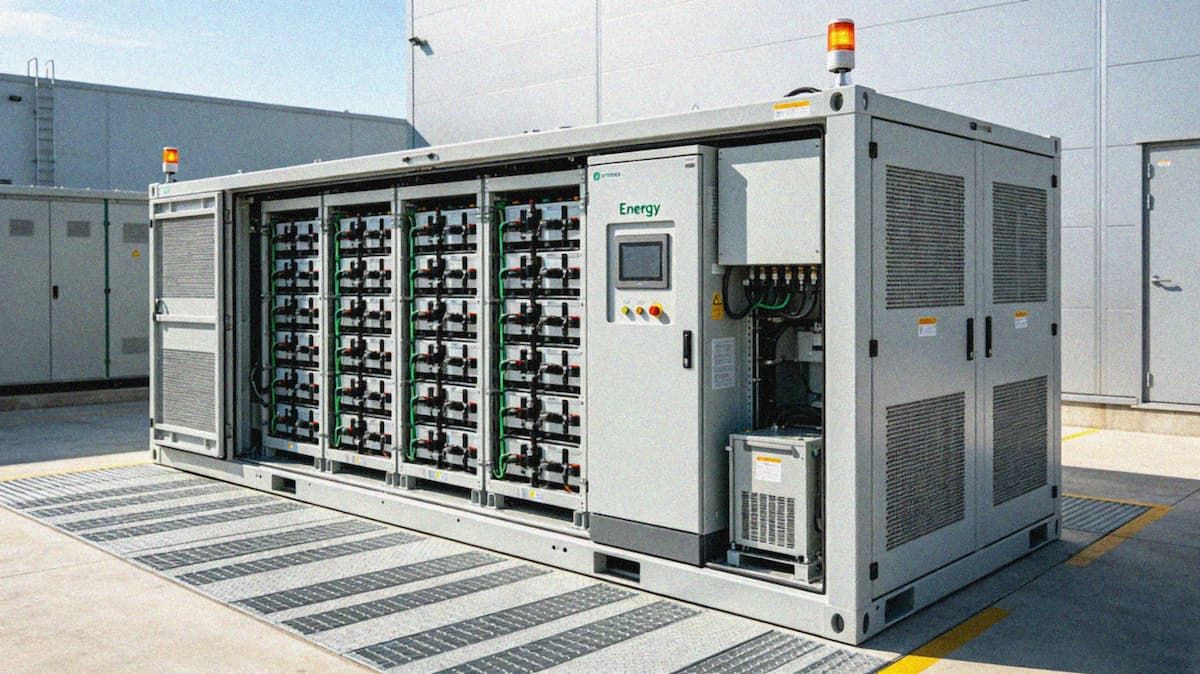
Over the past three years, global energy storage installations have grown at a sustained pace. According to industry estimates, new energy storage capacity additions worldwide exceeded 100 GWh in 2025, with China, Europe, and North America accounting for the bulk of the growth. Energy storage systems have moved rapidly from demonstration projects to large-scale deployment, with application scenarios expanding from grid-side frequency regulation and peak shaving to commercial and industrial load shifting, residential storage, and microgrids. This growth in installed capacity has directly driven demand for upstream electronic hardware, and PCBs — as the physical platform for the three core electronic subsystems in every energy storage installation — have seen demand rise in parallel.
A complete electrochemical energy storage system contains three core electronic subsystems. The battery management system (BMS) monitors cell status, performs cell balancing, and executes safety protection. The power conversion system (PCS) handles bidirectional conversion between DC battery voltage and AC grid voltage, serving as the interface between the storage system and the utility network. The energy management system (EMS) coordinates the overall plant operation, manages charging and discharging schedules, and provides data logging and remote monitoring. Each subsystem has its own PCB design requirements, and at the system level they must work together reliably.
This article examines each of the three subsystems in turn — BMS, PCS, and EMS — discussing their respective PCB design considerations, then looks at the system-level challenges that arise when these subsystems must collaborate in a single installation. For PCB designers and energy storage system integrators, understanding the design logic and interdependencies at the circuit board level helps avoid common engineering problems during the project planning phase.
BMS PCB Design — The Specific Challenges of Stationary Storage
Stationary energy storage BMS designs share the same fundamental functions as automotive BMS units — cell monitoring, balancing, and safety protection — but the design parameters differ significantly. Voltage levels in energy storage systems typically range from 1000 V to 1500 V DC, with some large-scale projects moving toward 2000 V DC, well above the 400 V or 800 V platforms used in passenger and commercial vehicles. Series cell counts are also higher: a single storage container may have more than 200 cells in series, compared with roughly 100 in a typical passenger vehicle pack. From a safety standpoint, the total energy in a stationary installation is far larger than that of a single vehicle, so the consequences of thermal runaway are more severe and the BMS fault detection sensitivity and response speed requirements are correspondingly stricter. These differences translate directly into PCB design: larger creepage distances, more isolated communication channels, and tighter functional safety design.
The cell supervision controller (CSC) in a storage BMS operates on the high-voltage battery side, and communication between the CSC and the main controller must be electrically isolated. The isolation withstand voltage is determined by the system voltage — a 1500 V DC system typically requires isolation rated above 5000 Vrms. At the PCB level, isolation design includes placing a sufficiently wide isolation barrier (typically 3 mm or more) with no copper or traces in the barrier region, positioning isolation transformers or capacitors to meet creepage requirements, and using clear silkscreen markings in the isolation zone to aid manufacturing and inspection. Storage BMS CSCs are usually connected in a daisy-chain topology, with 20 to 30 boards on a single chain. The longer the chain, the greater the risk of signal attenuation and reflection, which places tighter demands on trace impedance control and length matching.
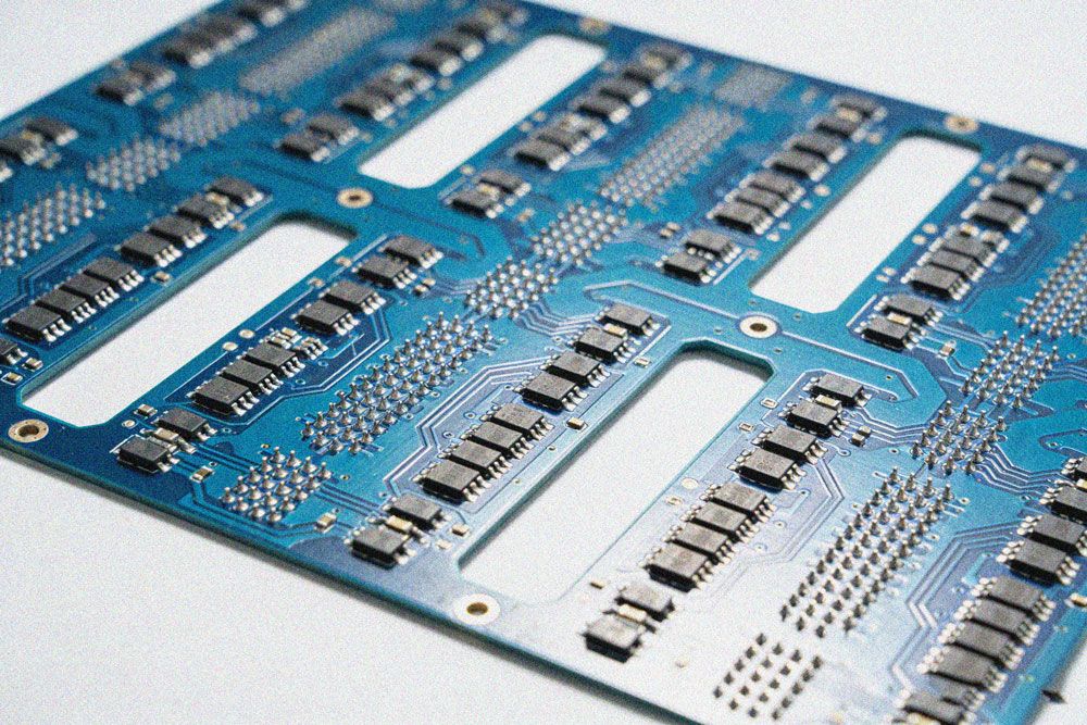
Storage BMS CSCs are typically 4–8 layer boards, with laminate selection balancing voltage withstand and cost. High-Tg FR-4 (Tg 170 or above) is the mainstream choice, capable of long-term operation inside battery enclosures where ambient temperatures can exceed 60°C. Differential trace pairs for sampling circuits need tight impedance control, usually within ±10%. Layout separation between analog sampling and digital communication zones, power supply decoupling, and trace width calculations for balancing current paths are all details that demand attention in storage BMS PCB design.
PCS PCB Design — High-Current Power Boards for Bidirectional Converters
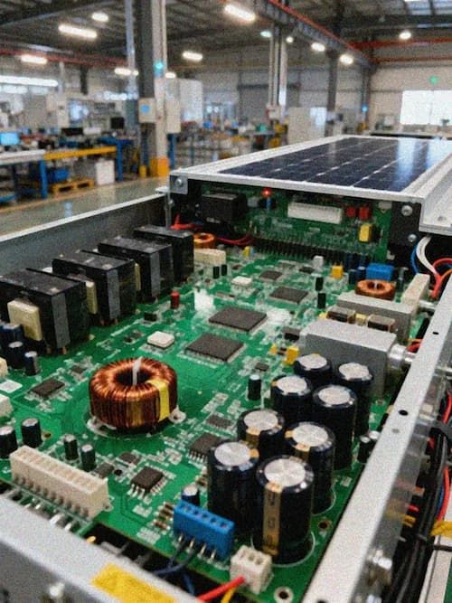
The PCS is the highest power-density subsystem in an energy storage installation, responsible for bidirectional energy conversion between the DC bus and the AC grid. In charging mode, the PCS rectifies AC power to DC for the battery; in discharge mode, it inverts battery DC power to AC for injection into the grid. The core power stage consists of a DC/DC converter and a DC/AC inverter, using IGBT or silicon carbide (SiC) power modules as switching devices. The power PCB must carry continuous currents above 100 A while withstanding high-frequency switching transients, making its design far more demanding than ordinary signal or control boards.
Carrying high current is the primary challenge for PCS power PCBs. Currents above 100 A require heavy copper construction, with copper foil thickness typically in the 4 oz to 6 oz range (140 μm to 210 μm), and some extreme applications need outer layers of 8 oz or more. Heavy copper fabrication introduces several difficulties: etch control for fine-pitch traces becomes less precise, layer-to-layer registration and lamination are harder to maintain when thick and thin copper are mixed in the same stack-up, and impedance calculation and signal integrity analysis become more complex. In addition to copper weight, high-current trace widths must be calculated from current density, typically held below 20 A/mm² to limit temperature rise. The interface between busbars and the PCB also needs careful design to avoid excessive contact resistance and localized heating.
The gate driver board is another critical PCB within the PCS. It generates the gate drive signals for IGBT or SiC modules, supplying sufficient peak drive current (SiC modules typically need 5–10 A) and precise dead-time control. The gate drive signals have fast edges (rise times in the tens of nanoseconds), so PCB layout must address signal integrity and EMC — drive traces should be short, differential, and symmetric to avoid parasitic inductance causing gate voltage oscillation. Thermal design is equally important for PCS power PCBs. Power device losses (conduction plus switching) generate heat that must be conducted through the PCB to the heatsink. Thermal via arrays, metallized thermal vias, and direct bonded copper (DBC) substrates are commonly used. PCB laminate thermal conductivity matters as well: standard FR-4 is around 0.3–0.4 W/m·K, while aluminum or ceramic substrates can reach 1–10 W/m·K.
EMS PCB Design — Multi-Protocol Communication and Control Boards
The EMS acts as the supervisory controller for the entire energy storage plant, coordinating the BMS, PCS, and external grid. The EMS controller collects real-time SOC and SOH data from the battery system, receives dispatch commands from the grid operator, executes charge and discharge schedules, and uploads operational data to a cloud-based monitoring platform. EMS control board PCB design emphasizes communication interface diversity and real-time data processing. A single EMS controller board typically integrates multiple protocols: Modbus RTU/TCP for BMS and PCS communication, IEC 61850 for grid dispatch system integration, Ethernet for local HMI and remote monitoring, and CAN bus for fast protective interlocking with power equipment.
Integrating multiple communication protocols on one board creates partitioning requirements for the PCB layout. Ethernet and IEC 61850 are high-speed interfaces that need attention to signal integrity and EMC; Modbus and CAN are lower-speed but still require isolation and noise immunity. Isolation between different communication interfaces is particularly important — the EMS controller must simultaneously connect to high-voltage-side equipment (indirectly through the BMS and PCS) and low-voltage-side equipment (monitoring platforms, dispatch systems), so isolation zones on the board must be clearly delineated. EMS control boards are usually 8–12 layer designs, with the higher layer count needed to accommodate the variety of communication interfaces and the MCU or DSP processing unit.
The EMS relies on accurate data from the BMS for battery state information, from the PCS for power and power quality data, and from environmental sensors for temperature and humidity. The accuracy of this data acquisition directly affects the quality of EMS dispatch decisions. Remote monitoring requirements also mean the EMS control board needs cybersecurity capabilities — encrypted communication, access control, and secure firmware update mechanisms — which translate at the PCB level into secure element integration and encrypted communication interface layout.
Collaborative System-Level Design
An energy storage system contains both high-power switching circuits (PCS) and sensitive analog sampling circuits (BMS) in close proximity, so EMC design is the first system-level challenge. IGBT and SiC modules in the PCS generate intense electromagnetic interference during switching (dv/dt can reach tens of kV/μs), which couples into the BMS sampling circuits and EMS communication links through both radiated and conducted paths. System-level EMC measures include placing shielding barriers between PCS power boards and BMS sampling boards, using twisted-pair shielded cable for BMS sampling lines, routing EMS communication cables away from PCS power busbars, and following single-point or hybrid grounding strategies to avoid ground-loop-induced noise.
Grounding design in energy storage systems must address both safety grounding and EMC grounding. Safety grounding requires all metallic enclosures and accessible parts to be reliably bonded to protective earth. EMC grounding requires a rational connection between signal ground, power ground, and chassis ground to prevent noise from high-current return paths coupling into sensitive signal circuits. Communication bus sharing is another collaborative design issue — the BMS, PCS, and EMS must share a CAN bus or Ethernet network for data exchange, and bus arbitration, communication priority, and fault isolation strategies all need to be planned at the system level.
When a fault occurs, the BMS, PCS, and EMS must respond in a coordinated manner within milliseconds. For example, if the BMS detects cell overvoltage or overtemperature, it must send a shutdown command to the PCS over the communication bus and an alarm to the EMS; if the PCS detects abnormal grid voltage, it must disconnect from the grid and notify the EMS and BMS. This millisecond-level response requirement places demands on both the real-time performance of the communication bus and the reliability of the communication interface circuits on the PCB. At the PCB design level, fault protection signal traces should be kept short, and critical signals should have redundant routing so that basic safety protection remains functional even under single-fault conditions.
Closing
Energy storage system technology is evolving toward larger capacity and higher voltage levels. Battery system voltages are moving from 1000 V toward 1500 V, 2000 V, and beyond, while individual storage container capacities are expanding from 5 MWh to over 10 MWh. These voltage increases raise the bar for BMS isolation withstand voltage, PCS power device voltage ratings, and EMS insulation design. At the PCB level, higher voltages mean larger creepage distances and clearances, wider isolation barriers, and stricter withstand voltage test standards. At the same time, the growing adoption of SiC power devices in PCS applications, with their higher switching frequencies, introduces new challenges for PCB EMC design and gate driver board signal integrity.
As energy storage systems continue to scale and upgrade, PCB suppliers need to maintain several long-term capabilities. Experience in high-voltage isolation design — including isolation layout rules, withstand voltage test methods, and isolation material selection — is essential. Stable manufacturing capability for heavy-copper boards, with consistent etch precision and uniformity, is equally important. System-level EMC design support, with the ability to advise on PCB-level optimization for electromagnetic compatibility, rounds out the skill set. Suppliers that have built these capabilities will be well positioned to capture the sustained growth in energy storage system demand.