Edge AI is moving past the proof-of-concept stage and into scaled deployment. According to MarketsandMarkets, the global edge AI hardware market was worth USD 21.98 billion in 2024 and is projected to reach USD 58.9 billion by 2030, at a compound annual growth rate of 17.6%. Mordor Intelligence is even more optimistic about the edge AI accelerator segment, forecasting about USD 7.45 billion in 2025 and USD 35.75 billion by 2030, a 31% CAGR.
Behind that growth is a rapid expansion of use cases. Smart cameras, industrial inspection, robotics, automotive ADAS, and medical imaging equipment are all pushing AI inference down to the device, moving away from centralized cloud processing to gain lower latency, stronger data security, and less bandwidth consumption. The trend directly lifts demand for edge AI accelerators and brings a new set of engineering problems to hardware design and PCB manufacturing.
Edge AI Accelerator Technology Routes
Edge AI accelerators are not a single category but split into several technology routes by compute, power, and application. By chip architecture, they fall mainly into four families: GPU, ASIC, FPGA, and NPU.
In terms of market structure, ASICs held 47.2% of the edge AI accelerator market in 2024, reflecting the broader shift from general-purpose compute toward domain-optimized chips. PMarketResearch's figures for the AIoT edge AI chip market show a similar picture: ASIC at 43.89%, GPU at 24.56%, FPGA at 16.85%, and CPU and others at 14.70%.
Each architecture has its own emphasis. GPUs, with their mature CUDA ecosystem and strong parallel computing, dominate high-end edge AI; the typical example is the NVIDIA Jetson line, whose top Jetson Orin platform delivers 275 TOPS of AI compute, while the newer Jetson T4000 reaches 1,200 FP4 TFLOPS and is tuned specifically for robotics and edge AI inference.
ASICs and NPUs take another route. They are deeply customized for specific neural-network operations, giving them an advantage in compute per watt and making them a fit for power-constrained embedded systems. Google's Edge TPU delivers 4 TOPS of INT8 compute from a single chip at just 2 W, and Intel's Movidius Myriad X VPU likewise targets low-power vision applications such as smart cameras and drones. The drawback is limited flexibility: these chips usually support only specific frameworks and operators.
FPGAs sit between the two, offering some programmability while delivering better power efficiency than general-purpose CPUs or GPUs. AMD/Xilinx's Versal AI Edge and Kintex UltraScale+ families see wide use in industrial automation, communications, and automotive. Vivado 2026.1 has begun supporting the second-generation Versal AI Edge family, further extending adaptive-computing capability.
Mainstream Edge AI Accelerator Platforms
Selecting an edge AI accelerator platform means weighing compute, power, interfaces, software ecosystem, and supply chain maturity together. A few platforms stand out in the current market.
NVIDIA's Jetson line is one of the most complete edge AI ecosystems today, spanning a full product range from low power to high performance. Jetson Orin Nano suits entry-level edge AI, Jetson AGX Orin targets high-end robotics and autonomous driving, and the latest Jetson T4000 carries 64 GB of memory and supports real-time 4K video processing; paired with JetPack 7.2's Agentic AI toolchain, it is becoming one of the preferred platforms for embodied intelligence and on-device large-model deployment.
Qualcomm's QCS series has deep roots in mobile and IoT edge AI. The QCS6490 uses a 6 nm process and integrates a Hexagon DSP for 12 TOPS of INT8 compute, with 5G and Wi-Fi 6E support, and is widely used in industrial handhelds, smart cameras, and edge gateways. The higher-end QCS8550 targets edge computing platforms that need more AI compute, with up to 24 GB of LPDDR5X memory.
Google's Coral platform is built around the Edge TPU and emphasizes low power and rapid prototyping. An M.2 dual-Edge TPU accelerator module plugs directly into a motherboard to give an embedded system 8 TOPS of AI compute. Murata's Type1WV module measures just 15.0 x 10.0 x 1.5 mm, integrating the Edge TPU and a PMIC in a 120-pin LGA package for space-constrained devices.
AMD/Xilinx FPGA solutions have a distinct advantage in industrial and communications. The second-generation Versal AI Edge family integrates AI engines, ARM processors, and programmable logic, making it suitable for scenarios that must handle real-time control and AI inference at once. The Kintex UltraScale+ family is known for its balance of performance, power, and price, with product lifecycles typically exceeding 15 years, a fit for long-life industrial and automotive applications.
Hardware Architecture of an Edge AI Accelerator Module
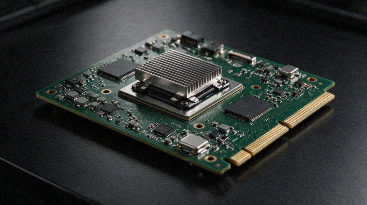
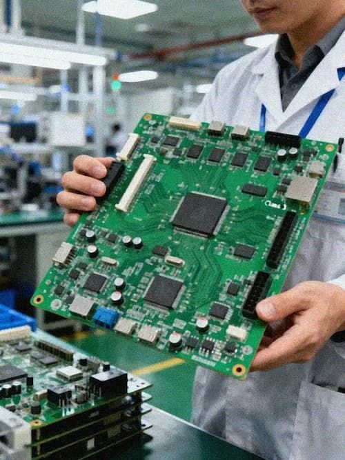
An edge AI accelerator module is a complete subsystem that, beyond the core AI chip, includes power management, clocking, thermal management, host interfaces, and telemetry. A self-contained Edge AI Accelerator Module typically consists of the following building blocks.
The AI accelerator chip is the core of the module and handles neural-network inference. Depending on positioning, compute can range from a few TOPS to several hundred TOPS. Memory needs to be placed tightly around the chip because AI inference is highly sensitive to memory bandwidth and latency. High-end platforms usually pair with LPDDR5 or LPDDR5X; the Jetson T4000 carries 64 GB, and the QCS8550 supports up to 24 GB of LPDDR5X.
Power management is another critical piece. An edge AI system typically needs four to eight independent voltage rails, covering core voltage, I/O voltage, DDR voltage, and various peripheral voltages. Point-of-load (PoL) regulators should sit as close to the SoC as possible, with industry practice keeping them within 10 to 15 mm to reduce power-distribution-network (PDN) impedance. Inference loads change quickly, and current transients cause voltage droop and noise, placing heavy demands on power integrity design.
Thermal design deserves equal attention. Concentrating high compute in a small volume creates localized hot spots. Thermal management has to be considered from the layout stage: use thermal via arrays to conduct heat from the bottom of the chip into internal power planes or the bottom layer, reserve heatsink contact paths for high-power components, and keep high-power parts away from sensitive RF or analog circuit areas. Layout and thermal simulation should iterate together, not be checked only at sign-off.
On interfaces, an edge AI accelerator needs to connect to the host system and external sensors. The host link is usually PCIe or USB, data-input interfaces include MIPI CSI, Ethernet, and USB 3.x, and there are also display outputs and industrial communication interfaces. Module design must also account for link enumeration, retraining, error reporting, and temperature and power telemetry.
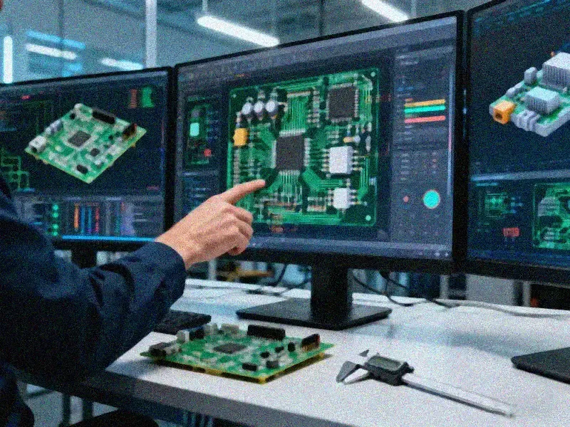
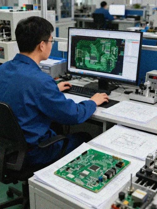
PCB design for an edge AI accelerator spans high-speed signals, power integrity, thermal management, and high-density interconnect, making it a classic multiphysics coupling problem.
High-speed interfaces are the first challenge to face. PCIe Gen4/5, LPDDR5, MIPI CSI, and USB 3.x all impose strict requirements on impedance control, trace length matching, crosstalk suppression, and reference plane continuity. With LPDDR5, for example, intra-byte skew must stay within 50 ps, which means physical trace length differences need to be controlled at the micron level. PCIe link stability, in turn, is tied directly to impedance mismatch, via stubs, and connector loss, and reflection is usually held within 3%.
Power integrity gets its difficulty from dynamic loading. Edge AI workloads fluctuate widely, and during an inference burst current can surge from a few amps to more than ten amps within a few nanoseconds. A poorly designed PDN leads to voltage droop, increased supply noise, clock instability, and memory data errors. In its edge AI PCB design guide, RapidCircuitry recommends providing ample decoupling capacitance for core and memory voltages and placing high-frequency decoupling capacitors as close to the chip power pins as possible.
Impedance control needs to be planned at the stack-up design stage. Single-ended signals are usually controlled to 50 Ω ±5% or ±10%, and differential pairs to 90 Ω or 100 Ω ±10%. In practice, designers use impedance calculators such as Polar SI9000, combined with laminate parameters, copper thickness, trace width and spacing, and dielectric thickness, to compute values precisely. For high-speed signals, the impedance discontinuity introduced by vias must also be addressed, with back-drilling used when necessary to remove via stubs.
Layer count and stack-up structure depend on signal density and impedance requirements. Edge AI accelerator PCBs typically run 10 to 12 layers, using an any-layer HDI structure for the highest interconnect density. Stack-up design has to balance signal, power, and ground layers so that every high-speed signal has a complete reference plane.
Key Manufacturing Considerations
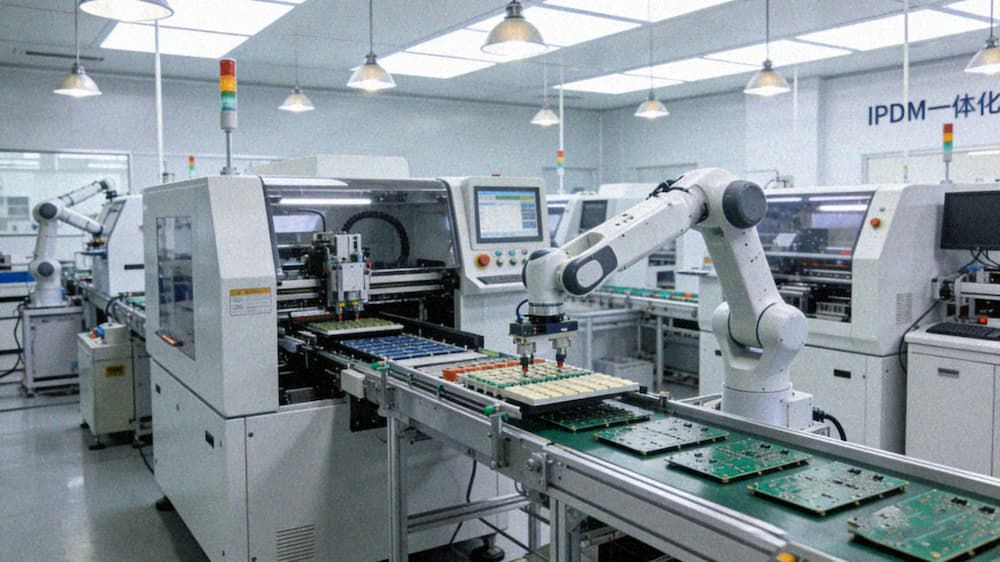
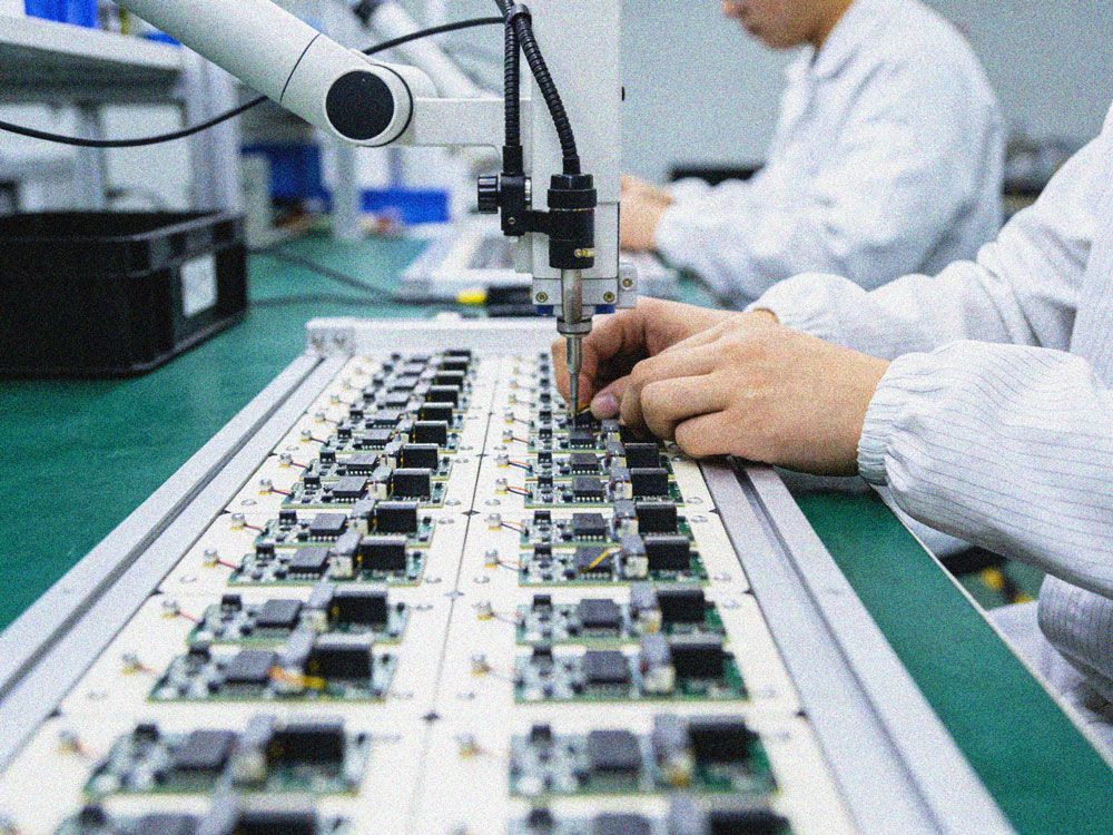
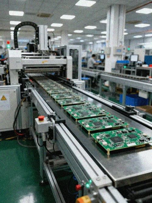
From a manufacturing standpoint, the process requirements for edge AI accelerator PCBs concentrate on three areas: HDI, impedance control, and material selection.
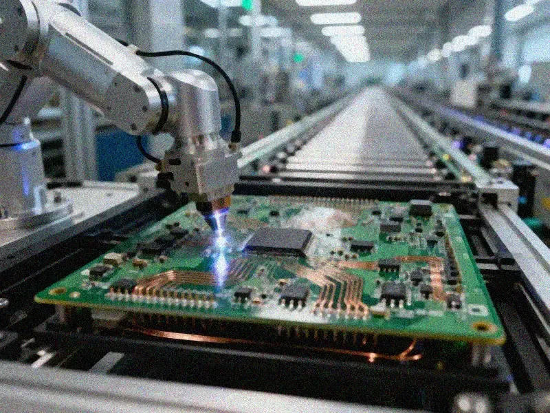
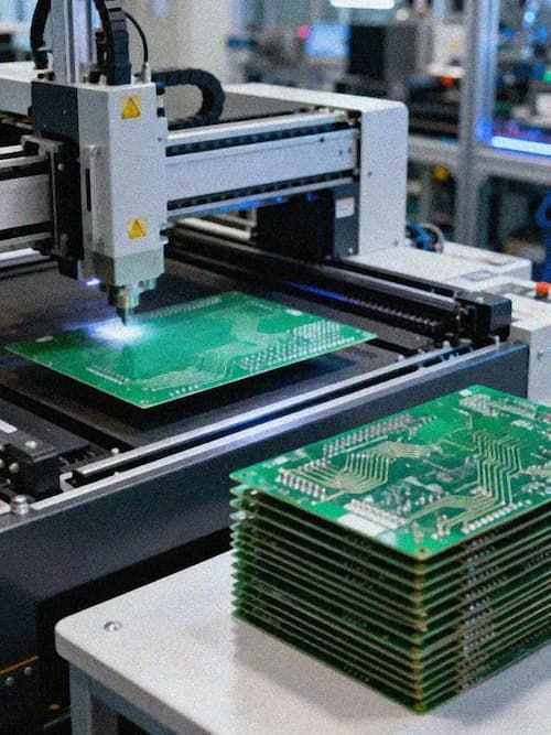
HDI (high-density interconnect) is a required process. Because AI accelerator chips usually come in BGA packages with 0.4 mm or finer pitch, traditional mechanical drilling cannot meet the fan-out requirements, so laser-drilled blind and buried vias are needed. Three-step blind and buried vias, 3/3 mil line width and spacing, 0.3 mm microvias, and via-in-pad are common configurations. Stacked-via technology can achieve higher density, but when two to three blind-via layers are stacked vertically they need resin filling for reinforcement to maintain structural reliability.
Consistency in impedance control directly affects yield. Beyond precise calculation on the design side, manufacturing must tightly control dielectric thickness, copper thickness, trace width, and etch factor. TDR (time-domain reflectometry) testing is the standard way to verify impedance control, and every batch needs sampling tests. For critical links such as PCIe, DDR, and high-speed serial interfaces, impedance deviation can directly cause link training failures or a higher bit error rate.
Material selection requires balancing performance and cost. Standard FR-4 suffers higher loss at signal frequencies above 10 GHz, so high-speed interfaces such as PCIe Gen4/5 and Ethernet running at 10G or above need low-loss laminates such as Rogers, Isola, or polyimide materials. At the same time, high-Tg (glass-transition-temperature) laminates are a baseline requirement for edge AI because chips run hot and the PCB must not soften or deform at elevated temperatures.
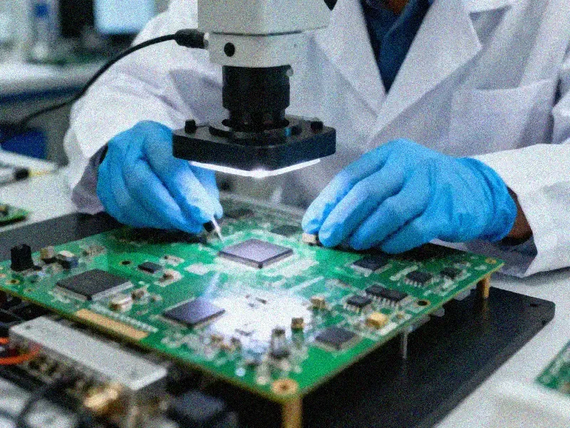
Test and validation cannot be skipped either. The PCIe and USB interfaces of an edge AI module need complete link testing, including enumeration verification, handshake stability, error-counter checks, and monitoring of link-retraining frequency. Voltage droop on the power rails under load, retimer signal quality, and reference-clock jitter all need to be verified one by one. These tests are not only functional validation but also a guarantee of long-term reliability.
Applications and Development Trends
The deployment scenarios for edge AI accelerators are expanding quickly. Smart cameras are one of the largest application areas today; DataIntelo data shows smart cameras account for about 27.9% of the edge NPU module market, worth roughly USD 1.34 billion in 2025. The global installed base of AI-enabled smart security cameras has already passed 770 million units, and beyond security, retail use cases such as footfall analysis, self-checkout, and inventory recognition are also growing fast.
Industrial automation and robotics form another important market. PMarketResearch data shows industrial automation and robotics account for about 34.4% of the edge AI accelerator card market, worth roughly USD 878 million in 2025. Factory visual inspection, predictive maintenance, and autonomous mobile robots are the main application directions. N-iX's industry analysis notes that in predictive maintenance, edge AI can judge equipment anomalies from sensor data in real time without waiting for a cloud round trip, significantly reducing downtime.
Automotive edge AI demand is also rising quickly. MarketResearchFuture data puts the 2025 automotive edge AI hardware market at about USD 4.7 billion. L2+ vehicles typically need 50 to 200 TOPS of neural processing, and L3 and above demand even more. Automotive scenarios impose far stricter requirements on functional safety, reliability, and temperature range than consumer-grade designs, adding extra constraints to hardware design.
Medical devices and on-device large models are two emerging directions worth watching. Medical scenarios demand real-time inference and local data protection, and edge AI's sub-10 ms latency and on-device processing fit those needs. On the other hand, with JetPack 7.1 beginning to support TensorRT Edge-LLM, running large language models and multimodal models at the edge is becoming a reality. This trend will further push up demand for edge AI compute and memory bandwidth, and will also raise new questions for PCB design.
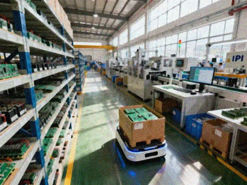
Designing edge AI accelerator hardware is a systems-engineering effort that spans chip selection, power design, thermal management, high-speed signaling, and manufacturing processes. For PCB manufacturers, HDI process capability, precise impedance control, and extensive high-speed board design experience are the baseline requirements for entering this market. KINGBROTHER has complete technical depth in high-layer-count boards, HDI manufacturing, and high-speed PCBs, and can offer edge AI accelerator customers one-stop manufacturing from prototype verification to volume production.