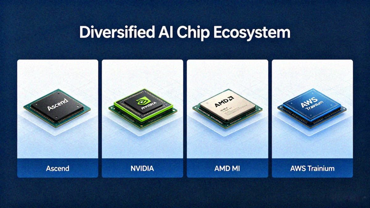
Over the past decade, CUDA has been almost equivalent to the underlying infrastructure for AI training. Through the deep coupling of GPUs and software stacks, NVIDIA has established a complete development tool chain and ecosystem, occupying a dominant position in the field of AI training. The situation has changed significantly in the past two years-platforms such as Huawei Ascend, AWS Trainium, and AMD MI series have matured rapidly, each forming available software stacks and hardware solutions. TrendForce data shows that the proportion of local chip purchases in the AI server market has increased to 40% in 2025. IDC predicts that global AI infrastructure investment will reach approximately US$75 billion in 2025. The successful operation of DeepSeek V4 on the Ascend platform further proves that the hardware dependence of AI training is migrating from a single platform to a multi-dimensional ecosystem.
The AI chip ecosystem is moving from unipolar to diverse
The historical status of the CUDA ecosystem is based on two foundations: the parallel computing capabilities of GPU hardware and the integrity of the supporting software stack. Since the release of CUDA 1.0, NVIDIA has continued to invest in building a developer ecosystem, making most AI frameworks and algorithm libraries give priority to supporting CUDA backend. This accumulation of software and hardware collaboration constitutes the threshold for other platforms to enter the field of AI training.
However, this pattern is being broken. Huawei Ascend gradually builds engineering capabilities in training and reasoning scenarios through the CANN (Compute Architecture for Neural Networks) software stack and Ascend series chips; AWS Trainium and Inferentia provide cost-optimized options for AI loads on the cloud; AMD MI300X has differentiated advantages in memory capacity and interconnection bandwidth. The maturity of these platforms makes NVIDIA no longer the only option for hardware selection for AI training.
The operation of DeepSeek V4 on the Ascend platform is a landmark event. As a model with a parameter size of one trillion, its training and reasoning have extremely high requirements on the computing power, video memory, and interconnection bandwidth of the underlying hardware. The ability to complete engineering verification on the Ascend platform shows that the platform's software stack and hardware capabilities have reached the threshold of supporting large-scale model training. For AI infrastructure planners, this means that the evaluation dimension of hardware selection needs to be expanded-in addition to NVIDIA's solutions, platforms such as Ascend and AMD also need to be included in the scope of technical evaluation and cost comparison.
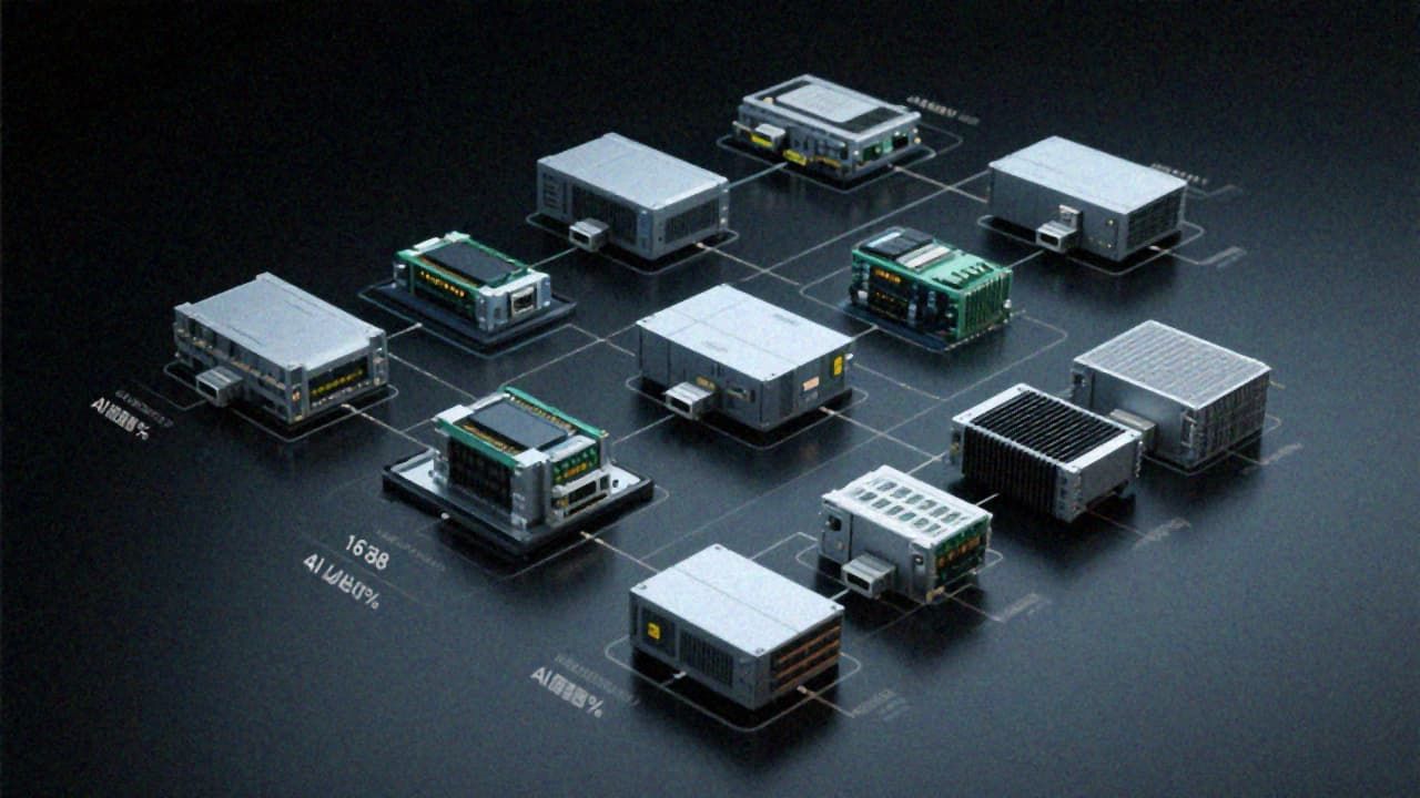
Judging from the coverage of processor platforms, a multi-dimensional ecological pattern has been formed. The ARM architecture covers processor platforms such as TI, NXP, RK, and HiSilicon. The GPU direction covers solutions such as Jetson, Horizon, and Edge10. The FPGA direction includes programmable logic devices such as ZYNQ7020. This parallel situation of multiple architectures puts forward new requirements for hardware design and adaptation.
The impact of diverse ecosystems on hardware architecture design
Different AI chips have significant differences at the hardware interface level. In terms of packaging form, GPU acceleration cards usually use PCIe Goldfinger interfaces with auxiliary power supply, while some ASIC chips may use custom on-board packaging or dedicated interconnection interfaces. In terms of interconnection protocols, NVIDIA uses NVLink and NVSwitch to achieve high-speed communication between GPUs, Tencent uses HCCS (Huawei Cache Coherence System) protocol, and AMD relies on Infinity Fabric. These protocols differ in rate, topology and latency characteristics, which directly affect the design of server motherboards and backplanes.
Differences in heat dissipation interfaces are also transmitted to the PCB design level. The air-cooling solution requires reserving the installation space and air duct layout for the radiator fasteners, while the liquid-cooling solution requires planning the location of the cold plate interface and pipeline direction. The TDP (Thermal Design Power Consumption) range of different chips varies greatly. The transition from several hundred watts to kilowatts has a direct impact on the PCB's thermal via density, copper filling strategy and dielectric material temperature resistance level.
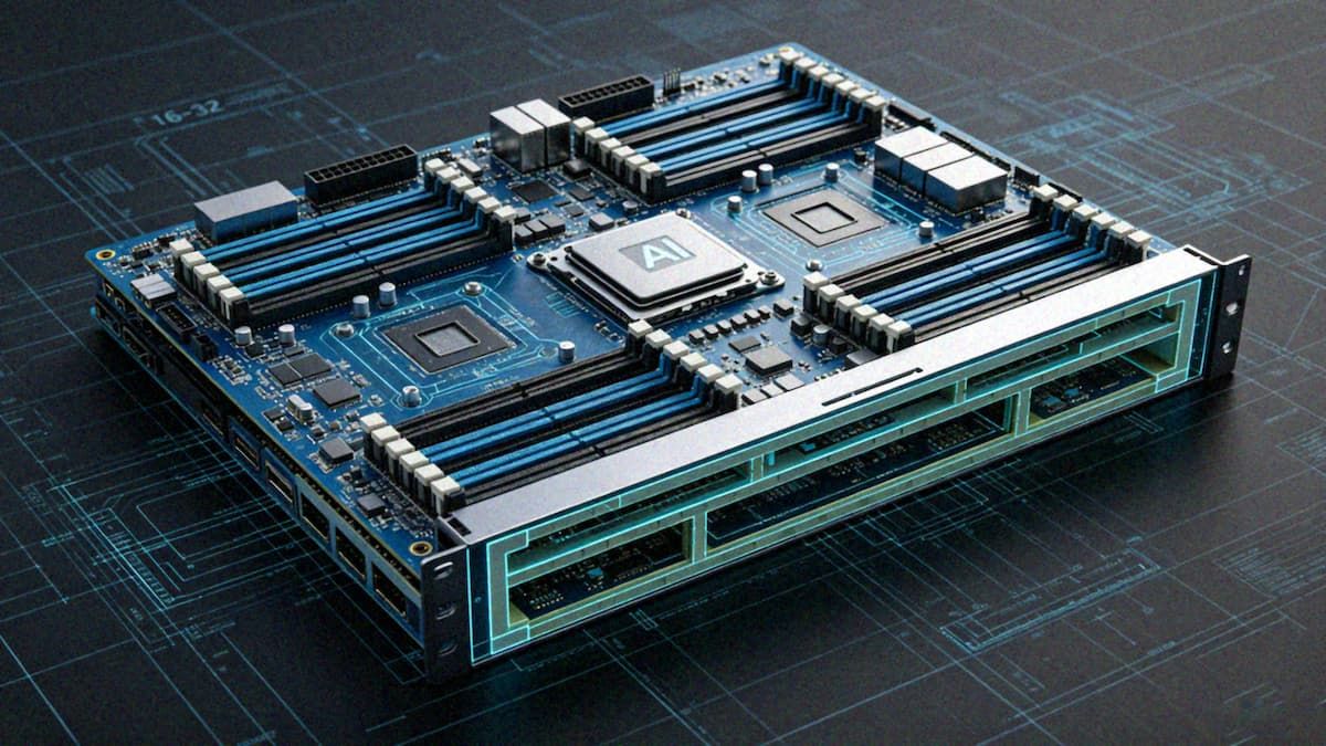
The core challenge facing server motherboard design is how to adapt the differentiated needs of different chips within limited board space. AI server motherboards usually adopt a 16-32-storey multilayer board design. The board is made of high-speed materials such as TU933 and ordinary FR-4. The minimum aperture reaches 0.2mm, the inner layer hole-to-line spacing is not less than 7 mils, and the line width and line spacing is controlled at 4.5/2.5mils. The delivery size is usually around 450x380mm, requiring multiple accelerator card slots, high-speed interconnect channels, power distribution networks and cooling interfaces within a limited area.
High-speed signal integrity is a key difficulty in motherboard design. Different interconnect protocols have different signal rate requirements. PCIe Gen5 reaches 32GT/s, while some dedicated interconnects may need to support SerDes rates of 56Gbps or even 112Gbps. The increase in signal rate directly tightens the accuracy requirements for impedance control-impedance deviation needs to be controlled within ±10% under mass production conditions, and ±5% during the sample stage. The back drilling process is used to eliminate the reflection effect of residual piles on high-speed signals, and its depth control accuracy directly affects signal quality. The accuracy control of metallized slots and crimp holes, and the resin filling process of high-density holes are all core technical capabilities in the manufacturing of AI server motherboards.
The need for flexibility in system-level architecture is becoming increasingly prominent. The modular design concept allows core computing modules to be reused and adapted to different chip platforms by replacing the acceleration clip board. The configurable power distribution network can adjust the power supply scheme based on the power consumption characteristics of different chips. Multi-protocol interconnection backplanes need to plan signal routing, impedance matching and crosstalk isolation schemes for different interconnection protocols during the design stage. These system-level design decisions directly affect the long-term evolution capabilities and operating costs of AI infrastructure.
Adaptation strategy for hardware supply chain
The formation of a diversified AI chip ecosystem has put forward higher adaptation requirements for the hardware supply chain. PCB design specifications, manufacturing process requirements and verification standards for different chip platforms are different, and the supply chain requires cross-platform technical accumulation and engineering experience.
Multi-platform PCB design capabilities are the foundation of adaptation work. Different chips have different requirements for PCB layers, plates, impedance control, and heat dissipation design. The design team needs to be familiar with the design specifications of each platform and the transition from the design input stage to the full-process coverage stage of Gerber output, including schematic design, layout planning, signal integrity simulation, power integrity analysis and other aspects, standardized processes and checklists for different platforms need to be established.
Rapid prototyping and verification capabilities can significantly shorten the hardware adaptation cycle for new platforms. In scenarios where chip platforms are switched or new platforms are imported, the hardware team needs to complete design modifications, prototyping, functional verification and reliability testing in a short time. Behind the rapid response capability is the accumulation and continuous iteration of the DFM (Design for Manufacturing) rule base-3.27 million certified materials and 2368 DFM rules, which can avoid a large number of manufacturing risks during the design stage and reduce the number of trial and error iterations.
The value of one-stop service lies in integrating the entire link of PCB design, manufacturing, and assembly, and reducing communication costs and coordination expenses for multi-platform development. Under the traditional model, design, manufacturing, and assembly may be undertaken by different suppliers, and problems in any link require coordination across suppliers. The one-stop model integrates the entire process under a single interface. Feedback from the manufacturing process can be obtained during the design stage, design data can be quickly retrieved during the manufacturing stage, and the bill of materials and quality records of the preceding links are directly used during the assembly stage. In this mode, the modular reuse rate can reach 68%, and the EMC test pass rate reaches 98.5%, which significantly improves the efficiency of multi-platform adaptation.
From the perspective of supply chain, behind the diversified ecological adaptation capabilities is long-term technical accumulation and engineering experience. 27 years of industry experience and the service records of more than 18000 customers show that various technical problems and boundary conditions have been encountered in a large number of projects. These experiences have finally been precipitated into design specifications, process parameters and quality standards. For teams planning multi-platform AI infrastructure, selecting hardware partners with multi-chip adaptation experience and one-stop service capabilities can effectively reduce adaptation costs and shorten the market cycle.
Hardware design methodology for diverse ecosystems
Modular design thinking is an effective strategy to deal with diverse ecosystems. The core computing module, power module, interconnection module, and heat dissipation module are independently designed and combined through standardized interfaces. When it is necessary to adapt to a new chip platform, only the corresponding computing module needs to be replaced or adjusted, and other modules can reuse existing designs. This idea can control the adaptation workload of the new platform within a reasonable range and avoid designing from scratch every time you switch.
Design-manufacturing collaboration is the key to avoiding engineering risks. The DFM rule base presupposes the constraints of the manufacturing process to the design stage, and the design team can get real-time feedback when laying out and routing-whether the trace spacing meets the etching process capabilities, whether the via density exceeds the capabilities of the drilling equipment, and whether the copper thickness distribution is uniform. These rules come from statistical analysis of a large amount of production data and verification results of process experiments, and can avoid potential manufacturing defects at the design source.
Future trends point to a higher degree of hardware abstraction and software definition capabilities. The hardware abstraction layer masks differences in underlying hardware through standardized driver interfaces, allowing upper-layer software to access computing resources of different chip platforms in a unified way. Software-defined hardware allows configuration and programming to adjust the behavior patterns of the hardware, such as the reconfigurable characteristics of FPGAs, the configurable parameters of ASICs, etc. The development of these technology directions will further reduce the complexity of adaptation under diverse ecosystems.
Heterogeneous computing requirements for edge AI scenarios are also growing rapidly. Edge AI chips such as DeepEdge10 provide 16TOPS of computing power and support the deployment of inference models on the edge side. Edge scenarios have special requirements for PCB miniaturization, low power consumption, and high reliability, and need to be treated differently from the high computing power and high interconnection bandwidth requirements of data center scenarios. AI industry applications have covered many fields such as large model training and reasoning, autonomous driving, robots, and smart agriculture and animal husbandry. Each field has different hardware needs, and the supply chain needs to establish design capabilities and process reserves for different scenarios.
IDC predicts that global AI infrastructure investment will reach approximately US$120 billion in 2028, and hardware demand in diverse ecosystems will continue to expand. For hardware supply chain planners, laying out multi-platform adaptation capabilities in advance, accumulating cross-platform engineering experience, and establishing a modular design system are reasonable steps to match the pace of this round of investment.