The explosion in demand for AI computing power is reshaping the PCB industry
The pace of global data center construction has accelerated significantly in the past two years. TrendForce data shows that the AI server market value will reach US$298 billion in 2025, and shipments in 2026 will increase by 28.3% year-on-year. This wave of computing power expansion is directly driving demand growth in the upstream PCB supply chain, especially for high-level and high-speed material products.
Prismark's PCB market report gives a more specific forecast: the global AI server PCB market will grow by more than 80% year-on-year in 2025, and the compound growth rate will reach 16.3% from 2024 to 2029. This growth rate is significantly higher than the overall level of the PCB industry, reflecting the rigid demand of AI computing infrastructure for high-end PCBs.
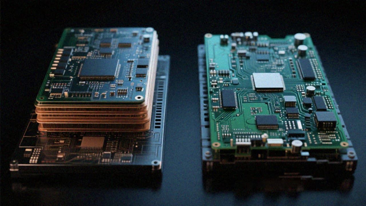
AI server PCBs are fundamentally different from traditional server PCBs. Traditional server motherboards are usually 8 to 16 layers, with signal rates below 10Gbps, which can be met by using conventional FR4 materials. AI server motherboards require 16 to 32 layers or even higher, and the signal rate evolves towards 56Gbps and 112Gbps. High-speed and low-loss materials such as TU933 + must be used for the board. The delivery size has also been expanded to 450×380mm, placing higher requirements on manufacturing equipment and process capabilities.
Technical thresholds and design challenges for AI server motherboards
High-level digital design is the primary feature of AI server PCBs. Mainstream AI server motherboards adopt a 16 to 32-layer structure, and some high-end accelerator cards have evolved to a 56-layer structure. The engineering challenges brought by the increase in the number of layers are manifold: the requirements for inter-layer alignment accuracy are narrowed, the increase in the number of lamination leads to the amplification of cumulative errors, and the increase in the density of inner layers increases manufacturing difficulties. According to industry data, the sample capacity of FR4 type PCB has reached 72 layers, and the mass production capacity is 32 layers; HDI type samples can reach 30 layers of arbitrary interconnection, and the mass production is 26 layers of 4 stages.
High-speed signal integrity is another core challenge. The AI server motherboard needs to carry high-speed interfaces such as PCIe 6.0, DDR5/HBM, and 112Gbps SerDes. At 112Gbps, issues such as signal attenuation, crosstalk, reflection and jitter are significantly amplified. Industry data shows that the current sample capacity of PCB manufacturing already supports a signal rate of 112Gbps, and the mass production capacity is 25Gbps; the impedance control accuracy of samples can reach ±5%, and the mass production is ±10%. The realization of these parameters requires collaborative optimization of materials, design and processes.
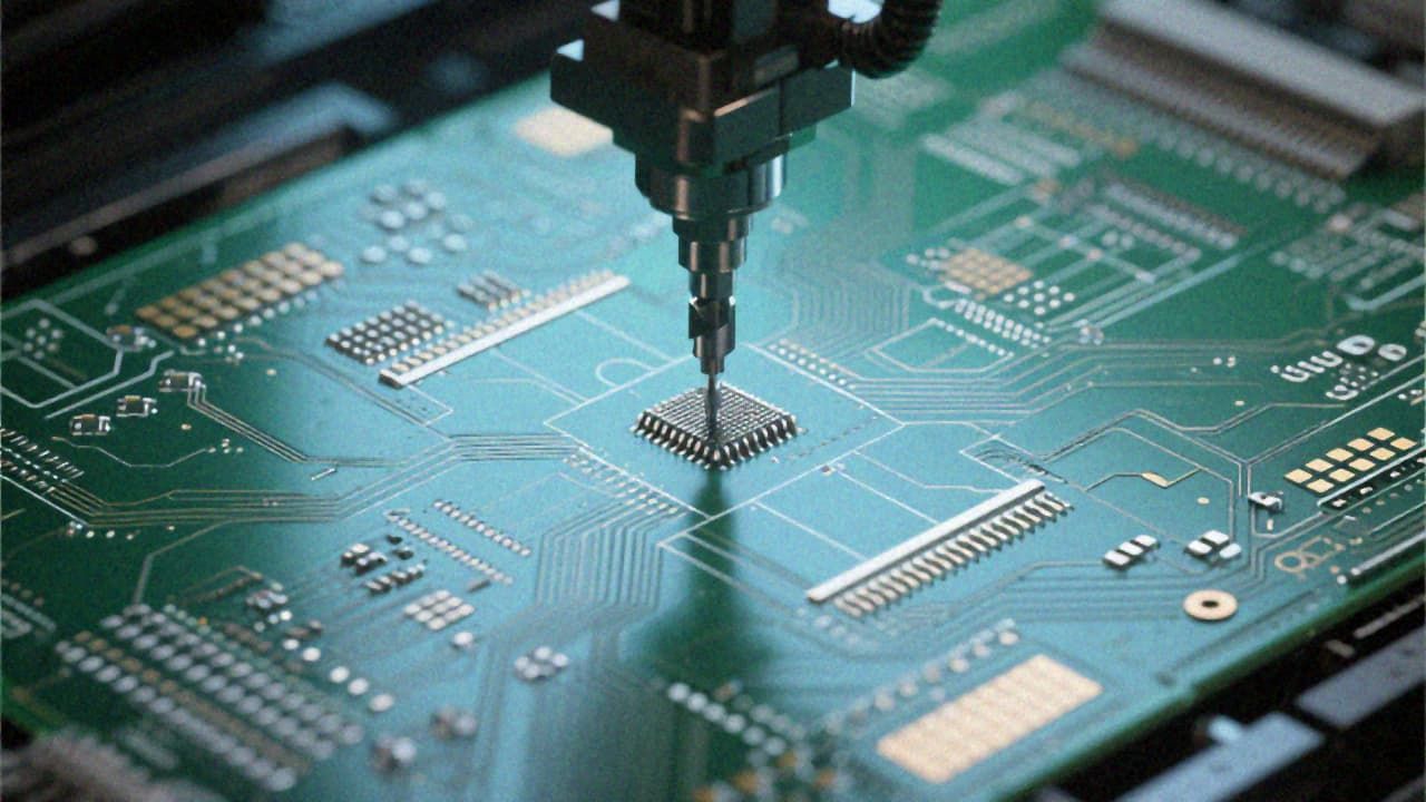
Specific to the process level, AI server PCB needs to solve a number of technical problems. The accuracy control of metallized slots and crimp holes directly affects the reliable contact of the connector; the multiple back drilling process is used to eliminate the impact of residual via piles on high-speed signals; the resin filling of high-density holes ensures the reliability of inter-layer interconnection. The minimum aperture reaches 0.2 mm, the inner layer hole-to-line spacing is no less than 7 mils, and the line width and line spacing is compressed to 4.5/2.5 mil-these parameters are almost never encountered in traditional server PCBs.
Thermal management and power density also require focused attention. AI server GPU power consumption has evolved to 700W or even 1000W, and liquid cooling solutions have gradually become mainstream. Under the trend of liquid cooling, PCBs need to adapt to cold plate installation, optimize heat flow paths, and increase the density of heat dissipation vias. Thick copper design has become a key means to deal with high currents. Industry data shows that sample copper thickness can reach 18OZ, and the mass production capacity is 6OZ.
Supply chain capacity gaps and structural contradictions
The contradiction between supply and demand in high-end PCB production capacity is emerging. Prismark data shows that the AI server PCB market will grow by more than 80% year-on-year in 2025, while the expansion rate of high-end PCB production capacity is significantly lagging behind. This imbalance between supply and demand has led to extended delivery times for some specifications, and the delivery times of some high-end AI server PCBs have been extended to 6 to 8 weeks.
The core reason for the capacity gap lies in structural imbalances. The production capacity of ordinary multilayer boards is relatively abundant, but the number of high-level boards and high-speed plate production capacity required for AI servers are seriously insufficient. Ordinary production lines cannot directly convert to high-end boards because of the fundamental differences in equipment, materials and processes between the two. Core equipment such as laminating equipment, back-drilling equipment, and impedance testing equipment for high-speed plates requires special configuration, with long investment cycles and high technical thresholds.
The material supply chain also faces bottlenecks. The supply of high-speed and low-loss plates (such as TU933 +, M6, and Megtron6) is concentrated in the hands of a few manufacturers. Delivery times for key materials such as special specifications copper foils and high-TG prepregs are also being extended. TrendForce data shows that the supply chain localization process in some regional AI server markets is accelerating, and the proportion of local chips has increased to about 40%, which has had a profound impact on the regional layout of the PCB supply chain.
Characteristics of suppliers with AI server PCB capabilities
When evaluating AI server PCB suppliers, technical capabilities are the primary consideration dimension. Specific indicators include: the highest number of layers (sample and mass production capabilities), the minimum line width and line spacing, impedance control accuracy, back-drilling process capabilities, and thick copper process capabilities. Taking industry data as an example, a supplier with 29 years of manufacturing experience has a FR4 mass production capacity of 32 layers, an HDI mass production capacity of 26 layers and 4 steps, a signal rate mass production support 25Gbps, and an impedance control mass production accuracy ±10%, and a thick copper mass production capacity of 6OZ. These parameters should be compared item by item with project requirements.
Quality system requirements are equally critical. The failure cost of AI server PCBs is extremely high, the value of a single motherboard may reach thousands of dollars, and the replacement cycle is long. Therefore, suppliers' yield levels, batch consistency, and traceability capabilities all need to meet stringent standards. Industry data shows that mature AI server PCB vendors typically establish a complete DFM rule base with more than 2000 rule entries, millions of certified materials, modular design reuse rates close to 70%, and EMC pass rates of more than 98%.
Ability to deliver is the third dimension of assessment. Capacity scale determines whether it can accept large orders, rapid response mechanism determines the ability to handle emergency demand, and flexible production capacity is related to the adaptability of multi-variety and small-batch orders. The iteration cycle of AI server products is shortening, the time window from design freeze to mass production delivery may be only 4 to 6 weeks, and the delivery elasticity of suppliers directly affects the progress risk of the project.
The construction of the supply chain of AI server PCBs takes time to accumulate. From material selection to process verification, from production capacity to stable quality, every link tests the supplier's engineering heritage. For teams planning the next generation of AI infrastructure, it is a reasonable pace to evaluate and target PCB suppliers with high-level numbers and high-speed signal capabilities.