Power design for AI accelerator boards is undergoing a quiet upgrade. As processor core counts and compute density climb, boards have to carry more current while supply voltages keep falling, and dynamic loads swing hard within microseconds. The older habit of treating power as a self-contained module no longer holds up under that combination of demands. Power integrity problems surface as system instability, fluctuating inference performance, and, at full load, crashes that are hard to reproduce.
PDN and the Power Tree
A 48V-to-point-of-load architecture is becoming the common choice for high-power accelerator boards. This factorized power approach uses a higher bus voltage to cut transmission loss, then converts to low-voltage, high-current rails close to the processor to reduce board-level drop. Running high current directly on 12V, by contrast, produces significant copper loss and forces board area and copper weight upward together.
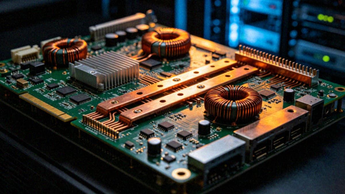
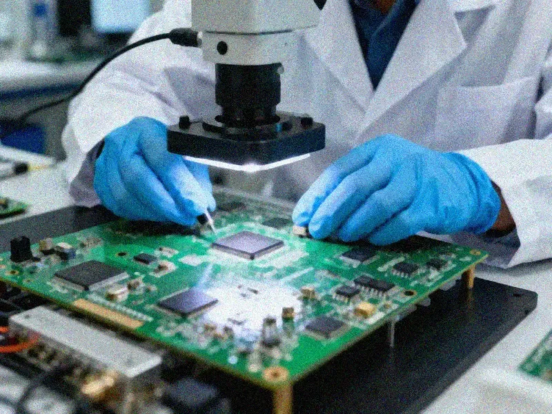
The power tree and decoupling are the most underestimated parts of PDN design. The area near the processor needs a dense population of decoupling capacitors, and low-ESL, low-ESR parts play a meaningful role in suppressing high-frequency noise and transient droop. Silicon capacitors from Murata and similar suppliers, with smaller packages and lower parasitics, offer a better option than conventional MLCCs in high-frequency decoupling. The placement of those capacitors, the number of vias, and the return path all shape the PDN impedance curve.
Thick Copper and Thermal Design
Current-carrying capacity against trace width and copper weight has to be calculated precisely. IPC-2152 provides the basis for that calculation, but real designs need an added temperature-rise margin on top of the computed value. Traces that are too narrow overheat under sustained load, accelerating insulation aging and solder joint failure; traces that are too wide consume board area, raise cost, and crowd out signal routing.
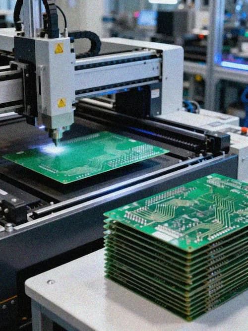
Copper weight follows the current requirement. One-ounce copper suits signal layers and low-current power layers, two ounces is the common compromise for robot and accelerator power boards, and three ounces or more serves the high-peak-current drive loops. The tradeoff is that heavier copper makes fine line and space harder to manufacture, so designers have to resolve current demand against process capability early. Power planes and vias usually matter more than traces, because multiple parallel vias can substantially reduce the current load on any single via, while plane splitting directly affects return paths and electromagnetic compatibility.
Manufacturing
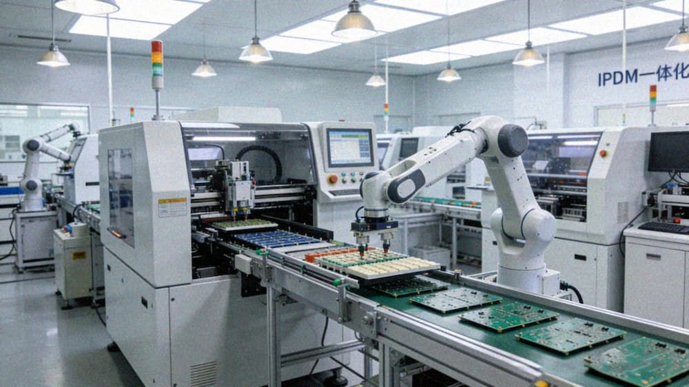
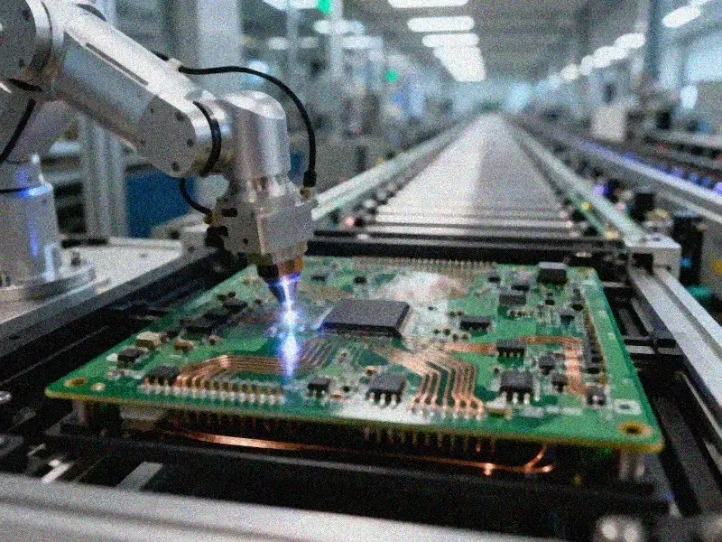
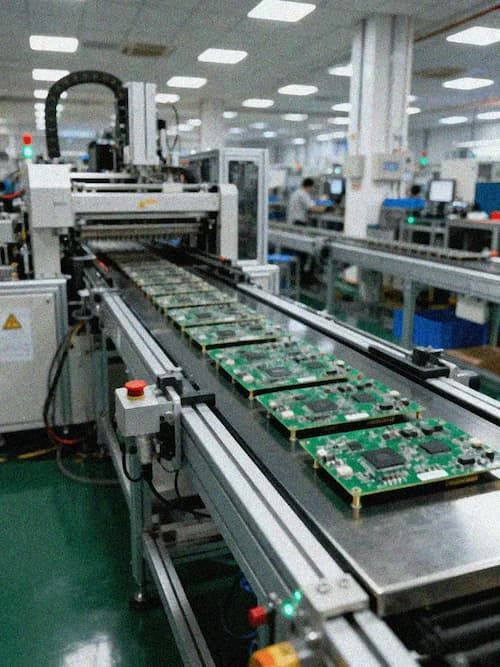
Whether a power design can be produced depends on the supplier's process experience with thick copper and high-thermal-conductivity materials. KINGBROTHER holds thick-copper and high-thermal-conductivity capability plus high-layer-count manufacturing; its AI server motherboard volume parameters cover 16-32 layers, TU933+ high-speed material, 0.2mm minimum hole, 4.5/2.5mil line/space, and 450x380mm delivery size. Those parameters define a realistic process boundary for taking an accelerator power board from design to production.
Closing
Design and manufacturing for AI accelerator power boards are tightening at the same time. PDN impedance, thick-copper current handling, the thermal path, and process capability all need to be brought into the design early. For teams planning a high-power accelerator board, moving power design ahead of the selection stage and aligning thick-copper and thermal-material capability with the manufacturer early is the most effective way to control rework risk; that early investment typically comes back in volume yield and lead time.