Overview
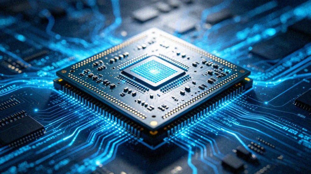
Power electronics systems serve as the core of energy conversion, voltage regulation, and power transmission across almost all industrial and consumer electronic scenarios, from small precision power supplies to large energy storage systems and high-voltage power transmission equipment. For these systems, PCB design directly determines the operational stability, energy conversion efficiency, and service life of the entire device. Unreasonable power electronics PCB design can easily lead to problems such as excessive component temperature rise, high-voltage breakdown, electromagnetic interference between power and control circuits, and even system-level failure causing safety risks. Our professional power electronics PCB design services cover the full end-to-end process from schematic optimization, stack-up planning, component placement and routing optimization, to multi-dimensional simulation verification, supporting a wide range of specialized material and process configurations to fully meet the stringent requirements of high-power, high-voltage, and harsh-environment application scenarios.
Technical Capabilities
We provide comprehensive technical support for power electronics PCB design, covering all core demands of different power application scenarios:
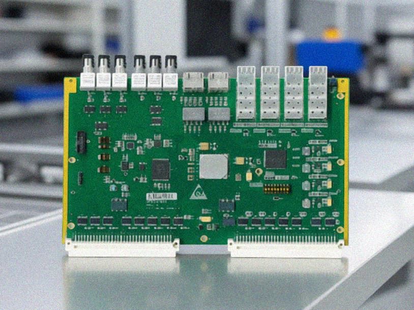
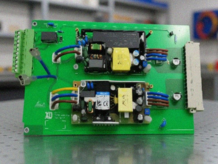
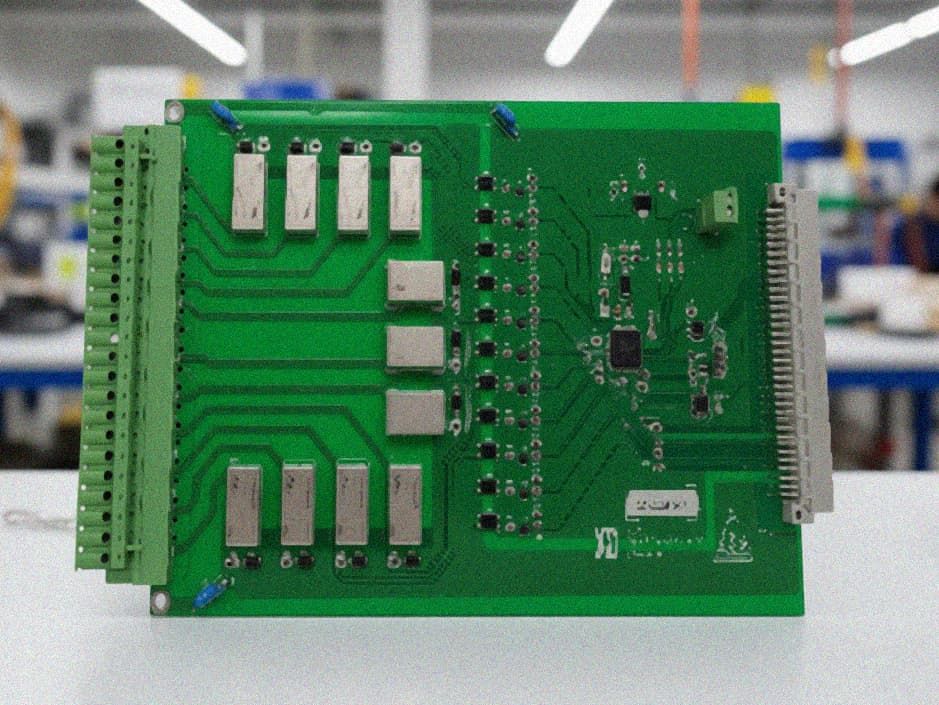
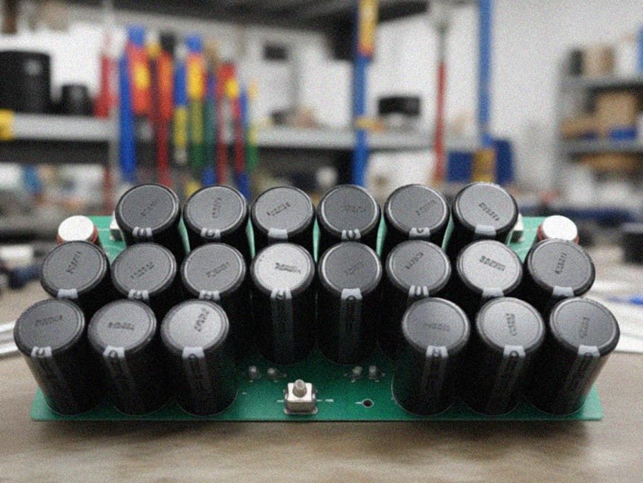
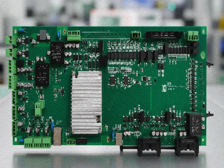
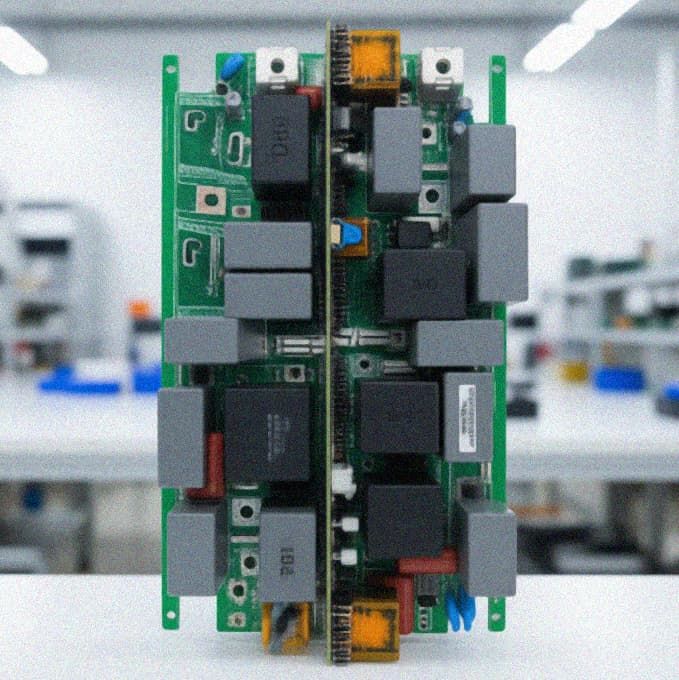
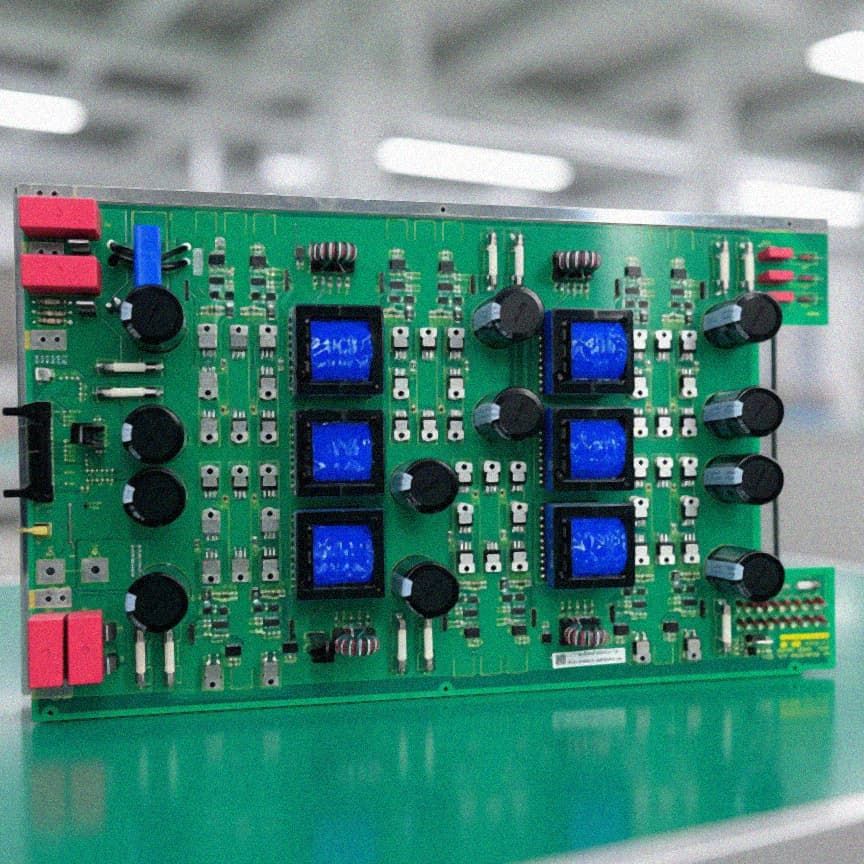
- Specialized Board Type Support: Covers design services for all common power electronics PCB types, including heavy copper boards (supporting 2oz to 10oz copper thickness configuration to improve current carrying capacity), high-voltage resistant boards (supporting 1kV to 10kV isolation design matching), alumina/aluminum nitride ceramic boards, rigid-flex integrated boards, high-frequency hybrid material boards, metal core substrates, buried copper block heat dissipation boards, and embedded component boards, adapting to diverse power application demands across different power classes.
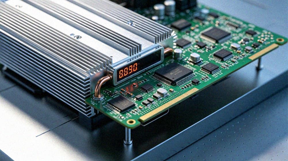
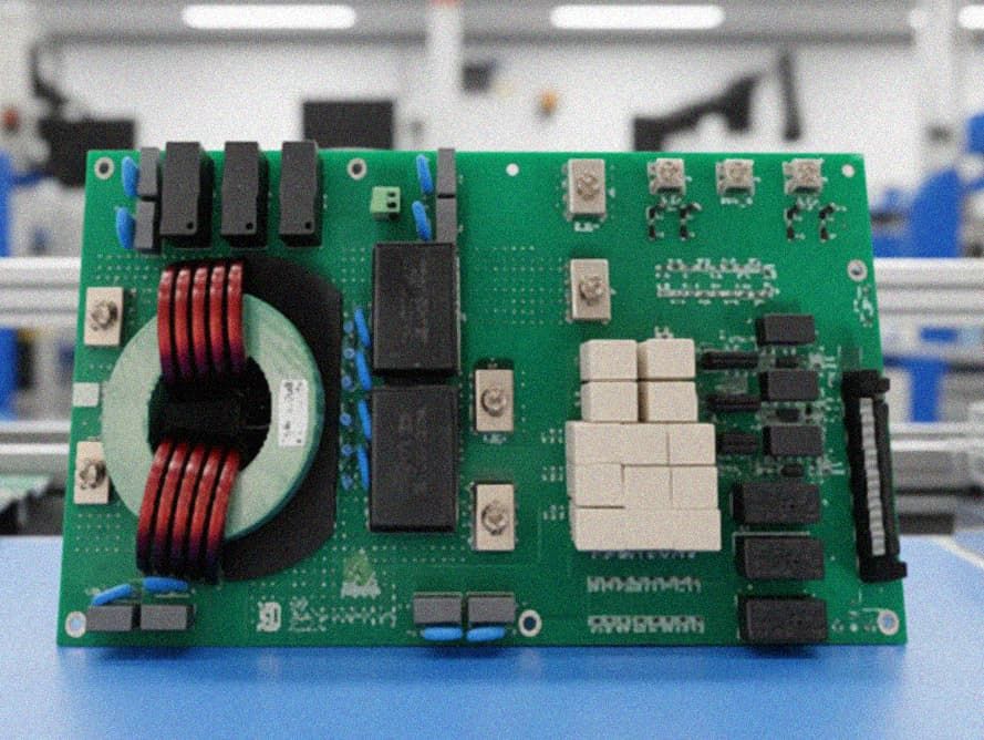
- High Efficiency Heat Dissipation Optimization: Provides targeted thermal management design schemes including embedded copper block heat conduction, metal substrate matching, thermal via array planning, and high heat dissipation material selection, reducing overall thermal resistance by up to 30% compared to conventional designs, ensuring stable operation of high-power core components such as IGBTs, thyristors, and power modules under long-term full-load working conditions.
- High Voltage Isolation and Protection Design: Supports targeted creepage distance and clearance optimization for high-voltage scenarios, high-insulation material configuration, and protective structural design, effectively avoiding risks of arcing, breakdown, and current leakage, fully meeting safety requirements of different voltage class power systems.
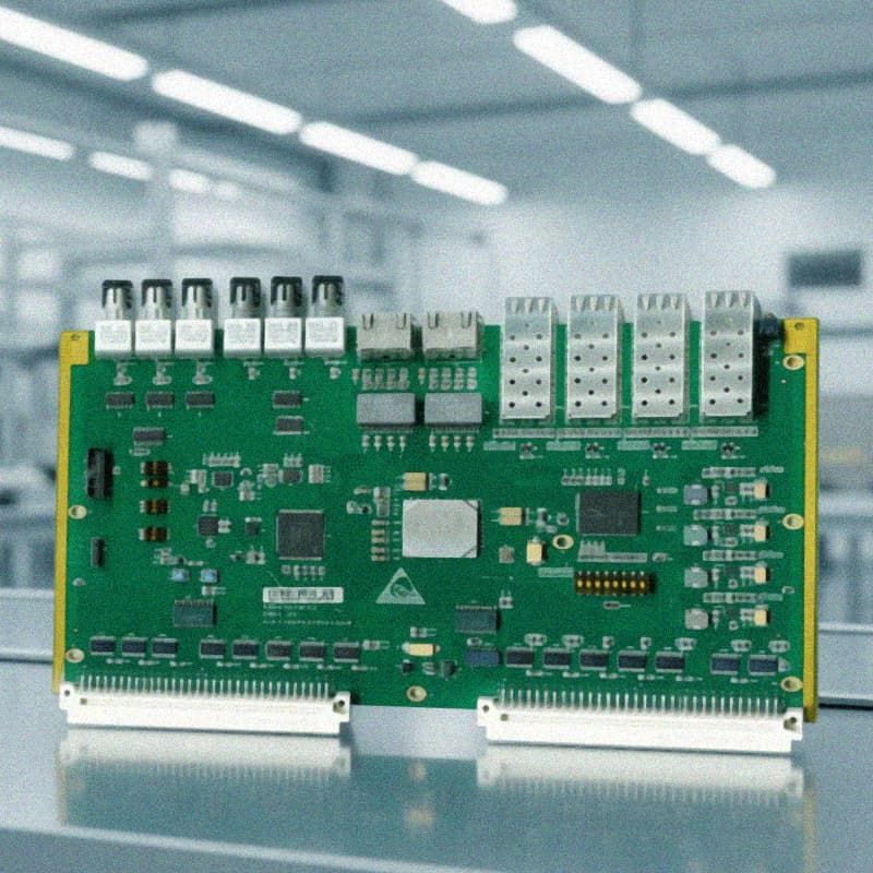
- Signal Integrity and Electromagnetic Compatibility Optimization: Implements layered routing planning for power signals, low-voltage control signals, and communication interfaces (including I2C, TDM, PCM, DC, and AC transmission interfaces), independent ground plane configuration, and precise impedance matching, reducing crosstalk between high-power circuits and low-voltage control circuits, ensuring stable signal transmission for acquisition, control, and communication units.
- Flexible Production Matching: Supports design adaptations for prototype verification, small and medium batch production, and large-scale mass manufacturing, compatible with HDI processes, mechanical blind and buried via processes, step board processes, and mixed pressure processes, effectively reducing iterative development cycles and cross-link manufacturing costs.
Quality Standards
All power electronics PCB design processes strictly follow IPC, UL, and relevant industry safety standards, with multi-layer verification mechanisms covering the entire design cycle:
- Schematic verification stage: Checks circuit logic correctness, power load matching, and protection circuit completeness, eliminating inherent design defects at the early stage.
- Pre-layout verification stage: Evaluates stack-up design rationality, impedance matching scheme feasibility, and thermal management effect through simulation, adjusting design parameters in time according to simulation results.
- Post-layout verification stage: Carries out DRC inspection, signal integrity simulation, EMC simulation, and thermal simulation, identifying potential design risks such as local overheating, signal attenuation, and interference before manufacturing.
- Post-production verification stage: Matches with electrical performance testing, high-voltage withstand testing, thermal cycle testing, and vibration testing, ensuring finished products meet operational requirements in -40℃ to +125℃ industrial-grade temperature ranges, and adapt to harsh working conditions such as high humidity, high salt spray, and strong vibration.
Applications
Power electronics PCB design solutions are widely applicable to multiple industrial and consumer power scenarios, including but not limited to:
- New energy systems: Energy storage integrated machines, photovoltaic inverters, wind power converters, and battery management systems (BMS)
- Industrial power equipment: High-precision power supplies, high-voltage power supplies, thyristor control units, frequency converters, and servo drive systems
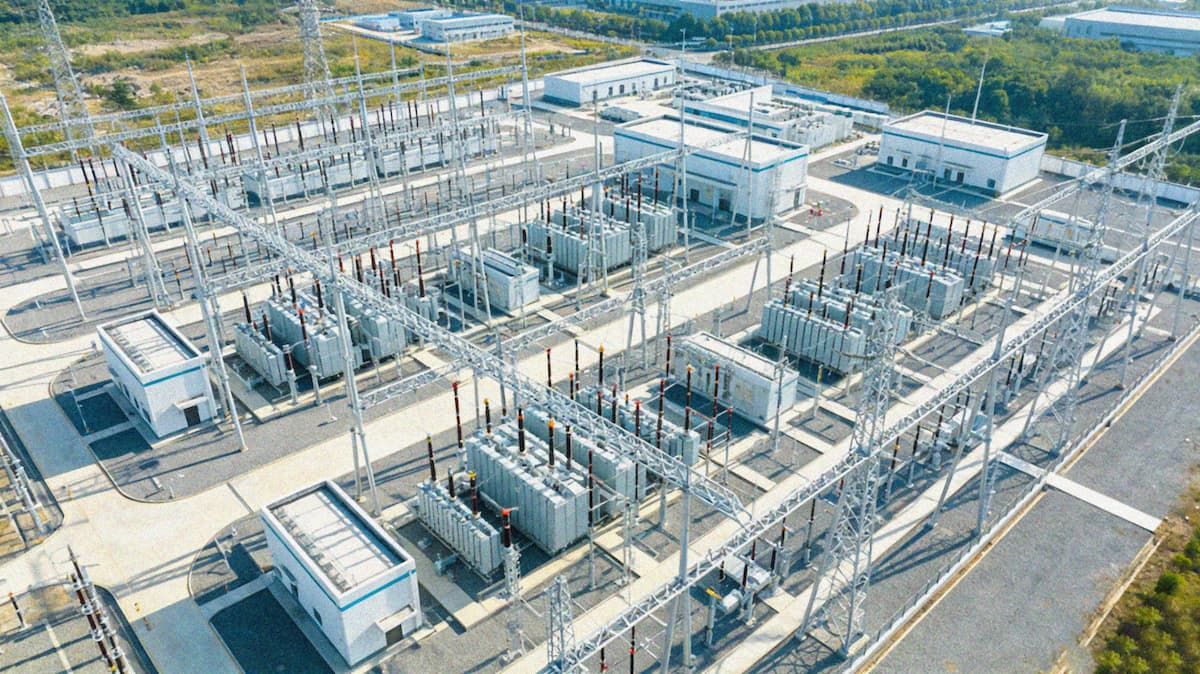
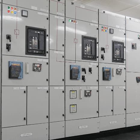
- Power transmission and distribution equipment: Converter valves, power distribution terminal units, and smart grid monitoring devices
- Automotive electronics: New energy vehicle on-board chargers, power distribution units, and motor drive control systems
- Intelligent terminal systems: Power boards, interface boards, acquisition main control boards, and signal processing boards for various industrial intelligent terminals
- Consumer electronics: Fast charging power modules, high-power household appliance power control units, and portable power supply systems
Key Advantages
- Full process coverage design service: Covers the entire R&D cycle from schematic design, component selection guidance, stack-up planning, layout routing, simulation verification, to manufacturing process guidance, reducing communication costs between design and manufacturing links, improving design feasibility and production yield by more than 15% on average.
- Customized configuration for scenario requirements: Provides targeted design schemes according to different application scenarios' power level, voltage class, working environment, and reliability requirements, flexibly balancing performance, cost, and production cycle demands for different project types.
- **Mature process compatibility: All design schemes are compatible with mainstream advanced PCB manufacturing processes, including buried resistance/capacitance/magnetic component processes, rigid-flex integration processes, high density interconnection (HDI) processes, and mixed pressure step processes, supporting rapid landing of innovative product designs.
- **Low risk iterative support: All designs undergo multi-dimensional simulation and verification before output, effectively reducing post-production modification risks, shortening product R&D cycles by 20% on average, and ensuring long-term stable operation of products with a design life of over 10 years for industrial grade applications.
Contact Information
If you have power electronics PCB design requirements, whether for prototype verification, small batch trial production, or large scale mass production, you can contact our technical team at any time. We will provide you with free pre-consultation, technical solution evaluation, and customized design services to fully meet your specific product development needs.