Overview
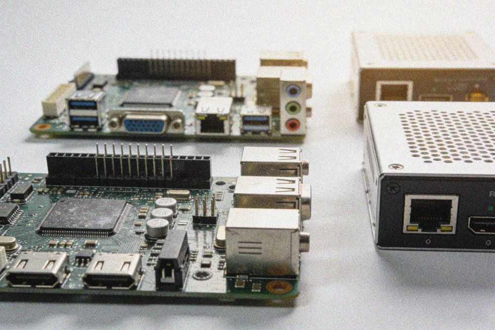
As consumer, industrial, and automotive electronic products continue to miniaturize while integrating more functional modules, HDI (High-Density Interconnect) PCB design has become a core requirement for modern electronic development. Unlike traditional PCB design, HDI design leverages micro-vias, fine line widths, and embedded component technology to achieve higher routing density, smaller form factors, and better signal performance, addressing common challenges associated with high-speed, high-component-count designs including signal crosstalk, impedance mismatch, thermal dissipation bottlenecks, and poor manufacturing feasibility. Professional HDI design services cover every stage of the development process from initial schematic review and stack-up planning to final DFM validation and production handoff, helping product teams balance performance, manufacturing cost, and time-to-market targets effectively. Whether for prototype verification or mass production deployment, optimized HDI design ensures products meet strict reliability, signal integrity, and regulatory requirements across diverse application scenarios.
Technical Capabilities
- Multi-Layer Stack-Up Design Support: Supports 2-30+ layer HDI stack configurations, including any-layer HDI (ALHDI) designs, with customizable layer arrangements for signal, ground, power, and embedded component layers to meet high-density routing and electromagnetic interference shielding requirements. Stack designs can be tailored to specific high-speed, high-power, or high-frequency performance needs.
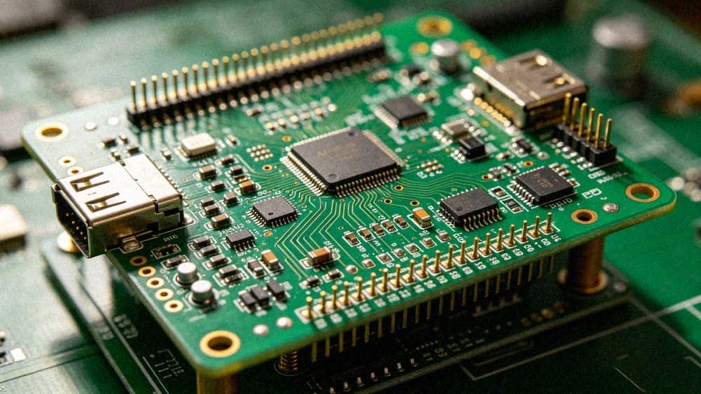
- Advanced Via Technology Optimization: Supports blind, buried, and micro-via designs with minimum via diameters down to 0.06mm, enabling high-density routing between layers without consuming valuable surface mount space, making it ideal for ultra-compact product form factors with strict size constraints. Via stitching and shielding configurations are also available to further improve signal integrity.
- Embedded Component Integration Capabilities: Supports design integration of embedded resistors, capacitors, copper blocks, ceramic substrates, and magnetic components directly into the PCB stack, reducing surface mount footprint by up to 30%, improving signal transmission stability, and enhancing thermal dissipation performance for high-power components.
- High-Speed Signal Integrity Optimization: Delivers precision impedance control with ±5% tolerance for 50Ω, 90Ω, 100Ω differential and single-ended signals, supporting high-speed interface transmission including I2C, TDM, PCM, DC/AC power networks, and high-speed backplane links to minimize crosstalk, attenuation, and signal reflection. Signal integrity simulation is conducted for all high-speed routing to validate performance before manufacturing.
- Rigid-Flex and Special Substrate Compatibility: Supports HDI design for rigid, flexible, semi-flexible, rigid-flex, metal core, ceramic, and high-frequency hybrid substrates, adapting to diverse application environment requirements for heat resistance, vibration tolerance, high-frequency signal transmission, and mechanical flexibility.
- DFM and Cost Optimization: Conducts comprehensive design for manufacturing (DFM) reviews at every stage of the design process, adjusting routing, stack-up, and material selections to reduce production complexity, improve production yield, and cut overall product lifecycle costs by 10-20% without compromising core performance targets.
Quality Standards
All HDI PCB design processes adhere to international industry standards and IPC guidelines to ensure design reliability and manufacturing compatibility:
- Complies with IPC-2221 generic printed board design standards, IPC-2226 HDI design specifications, and industry-specific standards for automotive, medical, and industrial applications including IATF 16949 and ISO 13485 alignment for relevant use cases.
- Design outputs include complete, standardized fabrication and assembly documentation, including Gerber files, stack-up diagrams, impedance control tables, BOM lists, and assembly guidelines to ensure seamless handoff to manufacturing teams and eliminate interpretation errors.
- Pre-production validation covers full signal integrity simulation, power integrity analysis, thermal simulation, and EMC pre-testing to identify and resolve potential performance issues before manufacturing, reducing design iteration cycles by up to 40% compared to non-validated designs.
- All design processes comply with RoHS, REACH, and other global environmental regulatory requirements, supporting unobstructed market access for end products in major global regions.
Applications
HDI PCB design solutions are widely applicable across high-density electronic product segments, including:
- Consumer electronics: Smartphones, wearable devices, tablets, mini-LED backlight displays, portable audio-visual equipment, and smart home terminals
- Industrial electronics: Industrial control units, edge computing nodes, high-speed backplanes, IoT sensor terminals, and industrial automation equipment
- Automotive electronics: Advanced driver assistance systems (ADAS), smart cockpit control units, in-vehicle infotainment systems, EV power management modules, and autonomous driving domain controllers
- Medical electronics: Portable diagnostic equipment, implantable medical devices, patient monitoring systems, and medical imaging components
- Communications equipment: 5G base station terminals, high-speed routers, optical module components, and satellite communication devices
- High-performance computing: AI accelerator cards, server motherboards, high-speed storage devices, and data center network equipment
Key Advantages
- End-to-End Design Coverage: Covers the entire HDI design lifecycle from schematic review, stack-up planning, component placement, routing optimization, simulation validation, to DFM review, eliminating cross-team communication gaps and reducing overall project turnaround time.
- Customized Performance Tuning: Adjusts design parameters based on specific product performance requirements, including thermal management optimization for high-power devices, vibration resistance design for industrial and automotive applications, and high-frequency signal tuning for communications equipment.
- Manufacturability Guarantee: All design outputs are validated for compatibility with mass production processes, including laser drilling, LDI direct imaging, and embedded component fabrication processes, ensuring over 95% production yield for mature, optimized designs.
- Cost-Effective Solution Delivery: Balances performance requirements with material and production cost inputs, recommending optimal stack-up configurations, via structures, and material selections to reduce overall product costs without sacrificing performance or reliability.
- Flexible Service Scaling: Supports design requirements for prototype low-volume validation, mid-volume trial production, and high-volume mass production, adapting to different project stages and volume demands for both startup and enterprise clients.
Contact Information
If you have HDI PCB design requirements for your electronic product development projects, please reach out to our technical team with your design specifications and performance goals. We will provide you with customized design solutions, free DFM feasibility evaluations, and professional technical consulting support to help you bring high-quality, high-performance electronic products to market efficiently.