Overview
Energy measurement PCBs are the core hardware foundation for accurate power data collection, transmission, and analysis across residential, commercial, industrial, and grid-level applications. Even minor deviations in PCB performance, including signal attenuation, impedance mismatch, or poor heat dissipation, can lead to significant metering errors, revenue loss for energy operators, or even stability risks for power distribution systems. Our energy measurement PCB solutions cover the full process from design optimization, material selection, precision manufacturing, to full-scope reliability testing, addressing core industry pain points such as electromagnetic interference resistance, wide temperature range operation, high current carrying capacity, and long-term outdoor stability, to meet the strict performance requirements of various energy measurement scenarios.
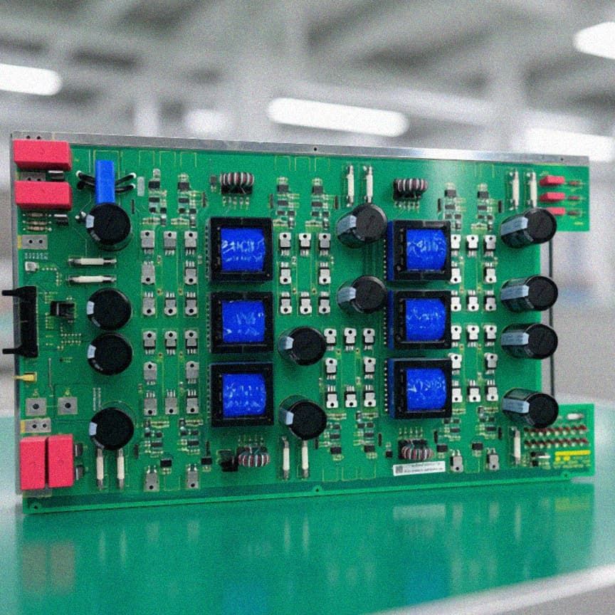
Technical Capabilities
- Diverse PCB Type Support: Covers single-sided, double-sided, 2-32 layer multilayer, HDI, rigid-flex, heavy copper (up to 12oz), high-frequency hybrid, ceramic, and embedded component PCBs (buried resistance, buried capacitance, buried copper block, buried ceramic) to adapt to use cases ranging from low-power residential smart meters to high-current industrial grid monitoring equipment.
- High-Precision Manufacturing Specifications: Supports minimum line width/line spacing of 2.0/2.0mil, micro vias as small as 0.06mm, 0.5 pitch minimum assembly accuracy, and SMD component packaging down to 01005 (0.3mm*0.2mm), meeting the high-density routing and miniaturization requirements of compact edge energy measurement terminals.
- Custom Size and Structural Adaptability: Accommodates conventional PCB sizes up to 600mm*450mm, component thickness ranging from 0.5mm to 3mm, and non-standard size configurations within semi-automatic printing equipment limits, adapting to both large centralized energy monitoring systems and small distributed metering nodes.
- Signal and Power Performance Optimization: Enables high-precision impedance control (error within ±5%) for DC/AC power circuits and I2C, TDM, PCM communication interfaces, reducing signal crosstalk and attenuation to ensure 0.1% or higher measurement accuracy for voltage, current, and power parameter collection.
- Embedded Component Integration Capability: Supports integration of buried copper blocks, buried ceramic substrates, and embedded passive components to improve heat dissipation efficiency, reduce PCB footprint by up to 30%, and enhance anti-electromagnetic interference performance for high-power, high-noise grid operating environments.
Quality Standards
All energy measurement PCB solutions adhere to strict quality control frameworks aligned with global power industry technical specifications. Products undergo full-process testing including signal integrity verification, EMC/EMI testing, high and low temperature cycle testing (-40℃ to +125℃), humidity resistance testing, salt spray testing, and current carrying capacity testing to ensure long-term stable operation in harsh outdoor, industrial, and residential operating environments. Manufacturing processes follow international quality management system requirements, with 100% electrical testing for all production batches, and full traceability of all raw materials and process parameters to support post-deployment compliance audits and maintenance. Products meet the 10-year+ service life requirements for fixed energy measurement infrastructure, reducing long-term operation and maintenance costs for energy operators.
Applications
Our energy measurement PCB solutions can be widely deployed across the following scenarios:
- Residential and commercial smart electricity meters: Compact, low-power PCB configurations for single-phase and three-phase smart meters, supporting high-precision metering, IoT wireless communication, and remote data transmission functions.
- Industrial energy management systems: Heavy copper and high-temperature resistant PCBs for industrial power monitoring terminals, adapting to high-current, high-noise factory floor environments to track real-time energy consumption of production equipment.
- Grid edge monitoring nodes: Rigid-flex and weather-resistant PCB designs for pole-mounted and substation energy monitoring devices, supporting stable operation in wide temperature, high humidity, and high vibration outdoor environments.
- New energy power generation measurement equipment: High-frequency and ceramic PCB configurations for solar inverters, wind turbines, and energy storage system power measurement modules, adapting to high-voltage DC and variable frequency operating conditions.
- EV charging station power metering units: High current carrying heavy copper PCBs for AC/DC charging pile energy measurement modules, supporting accurate billing and overload monitoring for 7kW to 350kW charging equipment.
- Building energy efficiency management systems: Multilayer HDI PCBs for centralized building energy monitoring terminals, integrating metering for electricity, water, gas and other energy sources to support intelligent energy scheduling.
Key Advantages
- Scenario-specific customization: Solutions can be tailored to meet unique requirements of different energy measurement use cases, from miniaturized personal energy monitoring wearables to large-scale industrial grid monitoring systems, with flexible adjustment of PCB material, stack design, and manufacturing process.
- Superior anti-interference performance: Optimized stack design with independent ground planes and optional embedded shielding layers to suppress electromagnetic interference from high-voltage power lines, wireless communication signals, and industrial equipment, ensuring measurement data accuracy even in complex electromagnetic environments.
- High cost efficiency: Supports both small-batch prototype manufacturing (1-100 units) for R&D verification and large-scale mass production (10,000+ units) for commercial deployment, with consistent quality control across all production volumes to balance performance and project budget.
- Full-process technical support: Covers end-to-end services from schematic review, stack planning, layout optimization, prototype fabrication, to mass production testing, reducing cross-stage communication costs and shortening product time to market by 20% on average.
- **Regulatory compliance alignment: All designs and manufacturing processes comply with global power industry safety and performance standards, including IEC 62052 for electricity metering equipment, supporting smooth product certification and market access for global deployment.
Contact Information
If you have customized requirements for energy measurement PCB solutions, including prototype development, mass production, or technical consultation for special application scenarios, please reach out to our technical support team. We will provide you with targeted solution recommendations, free design feasibility evaluation, and transparent quotation services based on your specific project parameters.