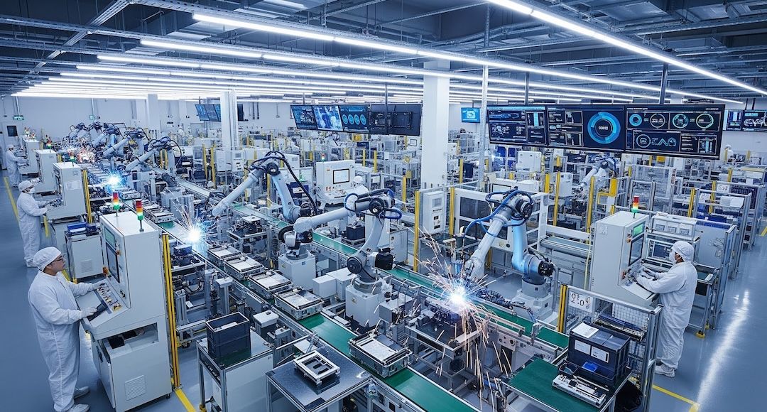
Overview
High-power electronic systems, industrial power supplies, automotive powertrains and renewable energy equipment face common core challenges including excessive current load, insufficient heat dissipation and mechanical stress damage under harsh operating conditions. Heavy copper PCB, manufactured with thick copper layers ranging from 3OZ up to 18OZ, effectively addresses these pain points by delivering superior current carrying capacity, thermal conductivity and structural stability, supporting reliable long-term operation of high-voltage, high-power electronic products. It eliminates the risk of copper trace fusing, board delamination and thermal failure under continuous high-load operation, becoming the preferred circuit board solution for high-power application scenarios.
Technical Capabilities
- Ultra-Thick Copper Layer Support: Supports copper thickness of 3OZ to 18OZ for both inner and outer layers, with 10-18OZ ultra-heavy copper configuration available to meet high-current transmission demands of up to several hundred amperes, eliminating risks of copper trace overheating and fusing under long-term high-load operation.
- Bump-Plated Copper Process: Adopts advanced bump-plated copper technology to achieve uniform copper thickness distribution across stepped structures, blind and buried vias, and high-density routing areas, ensuring consistent current carrying performance across the entire board without local performance degradation.
- Embedded Copper & Thermoelectric Separation Design: Supports embedded copper block and thermoelectrically separate copper-based board configurations, enhancing local heat dissipation efficiency by more than 60% compared to standard PCBs, effectively reducing junction temperature of high-power components such as IGBTs and power MOSFETs.
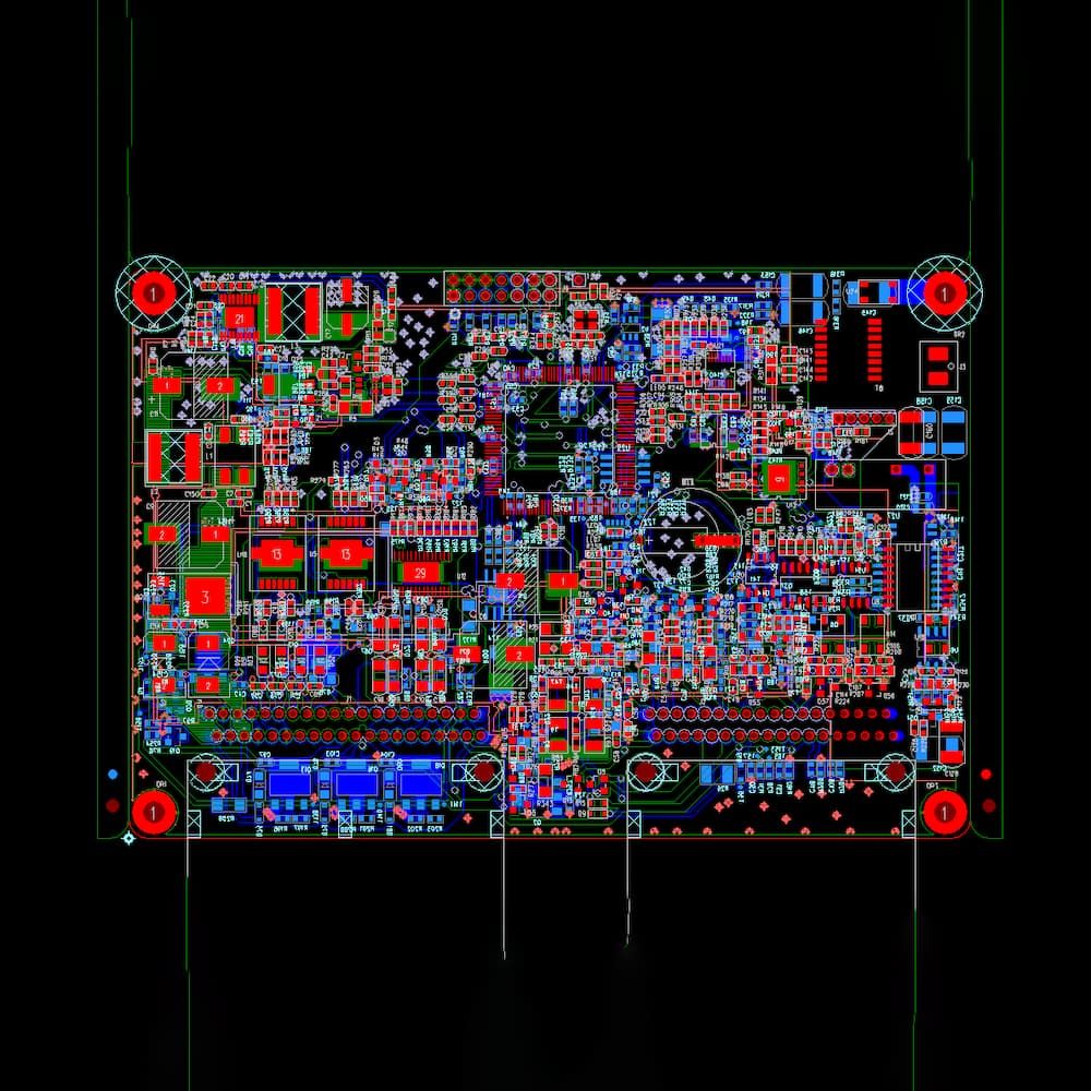
- High-Density Process Compatibility: Compatible with HDI processes, laser-drilled through holes, copper paste-filled vias, and multi-layer stackup designs of up to 24 layers, supporting mixed design of high-current power circuits and low-voltage signal circuits on the same board, reducing overall product size by 30% on average.
- Special Surface Treatment Options: Supports a full range of surface treatment processes including hard gold plating, soft gold bonding, and solderable metal plate coating, meeting the welding and connection requirements of high-power components and improving connection reliability under vibration and temperature cycling conditions.
- Customized Structure Support: Adaptable to special structure requirements including rigid-flex combination, metal core substrate, and embedded components, meeting the diversified design demands of different high-power application scenarios.
Quality Standards
Heavy copper PCB production strictly follows international IPC-6012, IPC-4101 and relevant industry-specific quality specifications, with full-process quality control covering raw material incoming inspection, process monitoring, and finished product testing:
- Raw material inspection: All copper foils and substrates pass UL 94V-0 flame retardant certification, with thermal expansion coefficient (CTE) precisely matched to copper layer parameters to avoid delamination under high temperature cycling of -40℃ to +125℃.
- Process control: Real-time monitoring of copper plating uniformity, line width tolerance, and via filling rate, with line width/space control accuracy of ±10% and copper thickness tolerance controlled within ±5% to ensure consistent electrical performance across all areas of the board.
- Finished product testing: All finished boards undergo 100% electrical continuity testing, high-voltage insulation testing, thermal shock testing, and salt spray corrosion testing, ensuring stable operation in harsh environments with high humidity, high salt and strong mechanical vibration, and meeting IP protection requirements for industrial and outdoor application scenarios.
Applications
Heavy copper PCBs are widely used in high-power, high-reliability electronic scenarios across multiple industries, including:
- New Energy Industry: Solar inverter controllers, wind power converter systems, energy storage battery management systems (BMS), electric vehicle charging piles, and on-board powertrain control units.
- Industrial Control Field: High-power switching power supplies, industrial servo drive systems, UPS uninterruptible power supplies, welding equipment control boards, and high-current power distribution modules.
- Automotive Electronics: Electric vehicle OBC (on-board charger) boards, high-voltage power distribution units (PDU), automotive electric drive control systems, and new energy vehicle battery management systems.
- Aerospace & Telecommunications: Base station power supply modules, satellite power distribution systems, radar high-power transmitter boards, and 5G/6G communication equipment high-current power units.
- Medical & Lighting Equipment: High-power medical laser equipment control boards, LED high-power drive circuits, and medical diagnostic equipment high-power supply modules.
Key Advantages
Compared with standard FR4 PCBs with 1-2OZ copper thickness, heavy copper PCBs offer the following core advantages:
- Superior Current Carrying Capacity: 10OZ heavy copper traces can carry more than 10 times the current of 1OZ standard copper traces of the same width, significantly reducing the size of power circuits and lowering overall product volume by 20-40%.
- Excellent Heat Dissipation Performance: High thermal conductivity of thick copper layers quickly dissipates heat generated by high-power components, reducing system operating temperature by 20-40% compared to standard PCBs, extending product service life by more than 2 times.
- High Mechanical Strength: Thick copper layers improve the structural rigidity of the board, reducing deformation under vibration, impact, and high temperature conditions, suitable for harsh operating environments with high mechanical stress.
- Reduced System Cost: Eliminates the need for additional heat sinks, busbars and cooling structures, reducing overall system BOM cost and assembly complexity, while improving system integration.
- Long-Term Reliability: Resists electrochemical corrosion and copper trace erosion under high voltage and high current conditions, reducing failure rates by more than 70% during long-term operation compared to standard PCBs, lowering later maintenance costs for end products.
Contact Information
If you have customized demands for heavy copper PCBs for high-power application scenarios, please contact our technical support team. We provide professional technical consultation, stackup design optimization, prototyping, and mass production services tailored to your specific application requirements, and can offer free pre-production technical evaluation for your projects to ensure the solution meets your performance and cost control needs.