Overview
RF & Microwave PCB is a specialized high-frequency circuit board designed to support signal transmission from 300MHz to millimeter wave frequency bands, addressing core pain points of conventional PCBs including high insertion loss, signal attenuation, crosstalk, and impedance misalignment in high-frequency operating scenarios. As the core carrier of RF front-end and microwave signal processing systems, these boards are optimized for consistent dielectric constant (Dk), low dissipation factor (Df), and high thermal stability, making them suitable for high-performance electronic systems that demand reliable low-latency, low-distortion signal transmission. The solution covers the full lifecycle from prototyping for R&D verification to mass production for commercial deployment, adapting to diverse technical and form factor requirements across industries.
Technical Capabilities
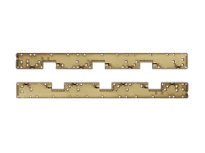
- Multi-Material Process Support: Compatible with pure PTFE, high-frequency hybrid lamination, FR4 mixed pressure, ceramic substrate, and rigid-flex composite materials, adapting to different frequency, loss, thermal conductivity, and structural flexibility requirements across use cases. Pure PTFE boards support up to 24 layers for prototyping and 16 layers for mass production, while high-frequency hybrid boards support up to 28 layers for prototyping and 20 layers for mass production.
- High-Speed Transmission Performance: Delivers maximum signal transmission rates of 112Gbps for prototyping and 25Gbps for mass production, meeting the high-bandwidth, low-latency transmission needs of 5G communication, millimeter wave radar, and high-speed wireless connection systems.
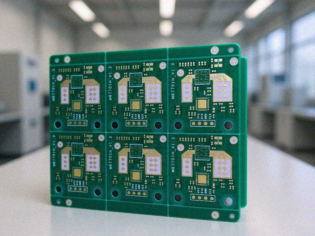
- High-Density Manufacturing Support: Supports HDI processes up to 28 layers with any-step interconnection for prototyping, and up to 20 layers with 4-step interconnection for mass production, catering to the high-density routing requirements of miniaturized integrated RF front-end modules. Rigid-flex RF PCBs support configurations of up to 30 total layers with 2 flex layers for prototyping, and up to 20 total layers with 12 flex layers for mass production.
- Diverse Form Factor Adaptation: Supports rigid RF PCB sizes up to 550mm1000mm for prototyping and 500mm550mm for mass production, with maximum board thickness of 12mm for prototyping and 6mm for mass production. Double-sided flexible RF PCBs support sizes up to 2000mm*200mm for prototyping, adapting to special installation requirements of curved and compact device structures.
- High-Precision Impedance Control: Achieves strict tolerance control for common RF impedance standards including 50Ω and 75Ω, with optimized etching and lamination processes to ensure impedance consistency across the entire board, minimizing signal reflection and insertion loss across the full operating frequency range.
Quality Standards
- Strict Performance Verification: All RF & Microwave PCBs undergo multi-dimensional performance testing before delivery, including insertion loss testing, return loss testing, impedance consistency testing, thermal cycling testing, humidity resistance testing, and vibration shock testing, ensuring stable operation in wide temperature ranges and harsh operating environments.
- Material Quality Control: High-frequency raw materials adopt full traceability management, with consistent Dk and Df parameters guaranteed across production batches to avoid performance fluctuations caused by material differences. Specialized material storage and processing procedures are implemented to prevent contamination and damage to high-frequency substrates during production.
- Industry Standard Compliance: Manufacturing processes fully comply with IPC-A-600, IPC-6012, and other international PCB industry standards, with zero tolerance for process defects that impact high-frequency signal performance such as etch back irregularities, via plating voids, lamination delamination, and surface roughness deviations.
Applications
RF & Microwave PCB solutions are widely applicable across high-frequency electronic scenarios, including but not limited to:
- **5G and Next-Gen Telecom Infrastructure: Used for 5G base station RF frontends, 5G couplers, power amplifiers, filter units, and millimeter wave communication modules, supporting high-bandwidth, low-loss signal transmission for wide-area 5G coverage and private network deployment.
- **Automotive and Industrial Millimeter Wave Radar: Applied to 77GHz automotive autonomous driving radar, industrial obstacle avoidance radar, traffic flow monitoring radar, and weather sensing radar, delivering stable signal performance in high-vibration, wide-temperature automotive and outdoor operating environments.
- **Aerospace and Defense Systems: Including satellite communication transceivers, radar warning systems, electronic warfare equipment, and drone navigation RF modules, with high resistance to extreme temperature fluctuations, low pressure, and radiation interference.
- **Medical and Industrial Microwave Equipment: Used for medical microwave ablation devices, industrial microwave heating equipment, and RF therapeutic instruments, meeting high safety and long-term stability requirements for continuous operation scenarios.
- **High-Speed Wireless Communication Devices: Including Wi-Fi 6/7 routers, satellite internet terminals, and industrial IoT gateways, supporting high-density signal transmission and low power consumption requirements for consumer and industrial wireless systems.
Key Advantages
- Customized Stackup Design Support: Provides tailored stackup planning based on application frequency, loss requirements, and form factor constraints, optimizing Dk consistency, ground plane shielding, and signal layer isolation to minimize crosstalk and insertion loss, reducing later R&D adjustment costs for customers.
- Scalable Production Capacity: Adapts to both low-volume fast-turn prototyping for R&D verification and high-volume stable mass production for commercial deployment, with consistent process control across production batches to ensure uniform performance of all delivered units.
- Low-Loss Process Optimization: Adopts specialized etching and surface treatment processes for high-frequency circuits, minimizing the impact of conductor surface roughness on signal transmission, improving overall RF system operating efficiency and reducing power consumption.
- Full Technical Support Coverage: Provides professional technical consulting from the early design stage to later mass production, including material selection guidance, stackup optimization, and design for manufacturing (DFM) suggestions, helping customers shorten product R&D cycles and improve market launch efficiency.
Contact Information
If you have customized RF & Microwave PCB requirements for your project, you can reach out to the technical support team for a free feasibility assessment and tailored solution quotation. Our team will provide professional technical consulting support throughout the entire project lifecycle from R&D verification to mass production, helping you resolve high-frequency signal transmission challenges and achieve optimal product performance.