Overview
Circuit board design is the core foundation of all electronic hardware development, directly determining product performance, reliability, manufacturability, and long-term operational stability. As modern electronic systems continue to evolve toward higher integration density, faster data transmission rates, and more specialized application scenarios, traditional generic design workflows often fail to address pain points including signal attenuation, crosstalk, impedance mismatch, thermal overheating, and low mass production yield. Our end-to-end circuit board design services cover every stage from schematic validation, stack-up architecture planning, placement and routing optimization, to pre-manufacturing compliance testing, delivering design solutions tailored to your specific performance, cost, and production volume requirements, while reducing development iteration cycles and lowering overall project costs.
Technical Capabilities
Our circuit board design services cover a full range of PCB configurations and specialized process requirements, with capabilities including:
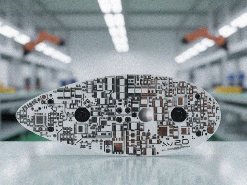
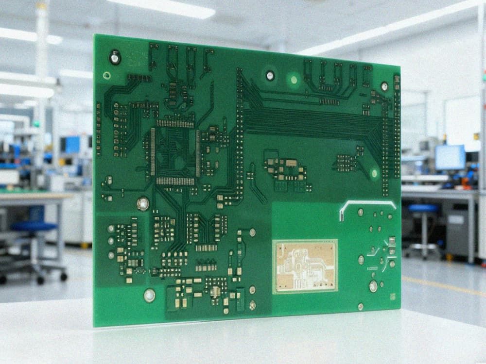
- Multi-Configuration Board Design Support: Covers single-sided, double-sided, and 2-64 layer multilayer boards, HDI boards, rigid-flex boards, semi-flexible boards, high-frequency hybrid boards, high-speed backplanes, metal core/metal substrate boards, ceramic boards, DBC ceramic boards, mini-LED backlight boards, high-resistance carbon oil boards, and IC packaging substrates, adapting to diverse form factor and performance requirements across application segments.
- Embedded Component Design Expertise: Supports design of embedded resistance, embedded capacitance, embedded magnet, embedded copper block, embedded ceramic, and embedded component boards, enabling 30% higher integration density than conventional surface mount designs, reduced signal path length, and improved electromagnetic interference (EMI) shielding for compact high-performance hardware.
- High-Speed & High-Frequency Design Optimization: Delivers impedance control accuracy of ±5% for 50Ω, 90Ω, and 100Ω differential and single-ended signals, supporting up to 800G high-speed optical module transmission, 6G antenna signal routing, and stepped high-frequency board stack-up planning, minimizing signal attenuation, crosstalk, and reflection loss for high-bandwidth data transmission scenarios.
- Specialized Process Design Compatibility: Supports design of stepped gold finger PCBs, bump-plated copper boards, thick GEM boards, thermoelectrically separate copper-based boards, and mechanical blind buried via configurations, aligning with specialized manufacturing process requirements for harsh environment, high-power, and high-reliability applications.
- End-to-End Design Validation: Includes pre-design schematic review, stack-up architecture optimization, placement and routing DFM (design for manufacturing) check, signal integrity (SI) simulation, power integrity (PI) simulation, EMC pre-compliance testing, and thermal performance simulation, eliminating design flaws before prototyping to reduce iteration cycles by up to 40%.
- Cross-Domain Interface & Integration Support: Compatible with common signal and power interfaces including I2C, TDM, and PCM for audio transmission, and DC/AC power supply routing, alongside electromechanical coordination design, appearance design alignment, structural reinforcement, and protective design integration to ensure seamless fit with end product enclosure and functional requirements.
Quality Standards
All circuit board design processes adhere to globally recognized industry specifications and regulatory requirements to ensure consistent reliability and manufacturability:
- Designs follow IPC-2221, IPC-2222, and IPC-7351 standards for generic PCB design, rigid board design, and surface mount land pattern design respectively, ensuring compatibility with mainstream PCB manufacturing and assembly processes worldwide.
- Design outputs are validated for mass production feasibility, with DFM checks aligned to standard manufacturing tolerances including line width/spacing as low as 2.0/2.0mil, micro-via diameters as small as 0.06mm, and layer alignment accuracy of ±0.02mm, avoiding design-related manufacturing defects.
- For high-reliability application segments, designs undergo additional stress testing validation including thermal shock cycling, vibration testing, and humidity resistance testing to ensure stable operation across -40°C to +85°C industrial temperature ranges.
- All design documentation is fully standardized, including Gerber files, BOM lists, assembly drawings, and test specifications, enabling seamless handoff to manufacturing teams without translation or adjustment gaps, and supporting RoHS, REACH, and conflict mineral compliance requirements.
Applications
Our circuit board design solutions are widely applicable across a full range of electronic hardware segments, including:
- Communication Infrastructure: 6G antenna modules, 800G high-speed optical modules, core network routing equipment, base station signal processing units, and 5G small cell terminal boards
- High-Performance Computing: Edge computing nodes, server high-speed backplanes, AI accelerator cards, data center storage equipment, and high-bandwidth memory interface boards
- Consumer Electronics: Mini-LED display backlight boards, smart wearable devices, high-end audio equipment, portable consumer terminals, and gaming hardware
- Industrial Electronics: Industrial control motherboards, power conversion modules, sensor interface boards, industrial automation control units, and harsh-environment monitoring equipment
- Automotive Electronics: In-vehicle infotainment boards, ADAS perception unit boards, automotive power management modules, and smart cockpit core control units
- Medical & Aerospace: Portable diagnostic equipment, low-power medical monitoring devices, aerospace telemetry modules, and high-reliability satellite communication sub-system boards
Key Advantages
Our circuit board design services offer distinct value for hardware development teams of all sizes:
- Manufacturability-First Design Logic: All design decisions prioritize mass production feasibility, with built-in DFM, DFA (design for assembly), and DFT (design for testing) checks at every stage, reducing prototyping iteration cycles by up to 40% and lowering mass production defect rates to below 0.1% for mature design solutions.
- Customized Configuration Flexibility: Supports modular design adjustments to balance performance, cost, and lead time requirements, with options for material selection including FR4, high-frequency PTFE substrates, ceramic substrates, and metal core substrates to align with project budget and performance targets.
- Full Lifecycle Technical Support: Provides ongoing design optimization support across prototype validation, small-batch trial production, and large-scale mass production stages, with dedicated technical teams available to resolve manufacturing compatibility issues, performance adjustment requirements, and functional upgrade requests in real time.
- Regulatory Compliance Alignment: All design outputs adhere to regional regulatory requirements for target markets, including FCC, CE, and UL certification pre-checks, reducing post-development compliance testing costs and accelerating time-to-market for end products.
Contact Information
If you have customized circuit board design requirements for specialized or high-performance electronic hardware, please reach out to our technical support team with your project specifications, performance targets, and volume requirements. We will provide a free pre-project technical evaluation, customized design proposal, and transparent cost quotation within 2 working days to support your product development roadmap.