Overview
The global medical wearable device market is expanding rapidly, covering consumer-level daily health monitoring and clinical-grade diagnostic and treatment auxiliary equipment, putting forward extremely high requirements for PCB design reliability, functional integration, and safety. Medical wearable PCB design is a specialized design service oriented to medical scenario requirements, addressing core pain points such as weak biological signal acquisition interference, limited device installation space, biocompatibility risks, and electromagnetic compatibility compliance. The design process covers the full chain from requirement analysis, schematic design, stackup planning, component placement and routing optimization, simulation verification, to prototype testing, fully adapting to the unique application scenarios of medical wearables that need to be in long-term contact with the human body and operate stably in complex environments. Unlike consumer electronic PCB design, medical wearable PCB design needs to balance multiple indicators such as signal accuracy, power consumption, volume, and safety, and meet the regulatory requirements of the medical device industry.
Technical Capabilities
- Low-Noise Signal Acquisition Optimization: For the acquisition requirements of weak biological signals such as ECG, EEG, SpO2, and heart rate variability (HRV) with amplitude lower than 1mV, the design adopts a 6-layer board architecture with independent separation of analog and digital ground planes, which can reduce cross-interference between digital circuit noise and analog acquisition links by more than 70%, effectively avoiding signal distortion and data deviation during biopotential collection. The design also includes pre-stage signal conditioning circuit matching, which further improves the signal-to-noise ratio of acquisition and meets the accuracy requirements of clinical-grade monitoring.
- Ultra-Miniaturization Design Support: Adopt high-density interconnection (HDI) and rigid-flex PCB design architectures, support micro-vias as small as 0.06mm and line width/line spacing down to 2.0/2.0mil, which can integrate more functional circuits in a limited space, reducing the overall volume of the PCB by up to 40% compared with conventional rigid board designs. The rigid-flex integrated structure eliminates the need for connector connections between boards, improving structural stability while further reducing the occupied space, which is very suitable for tight-fitting wearables and implantable medical devices with extremely strict volume requirements.
- Biocompatibility & Environmental Adaptation: Provide rigid-flex PCB paired with medical-grade nano biocoating solutions, which meet the long-term contact requirements with human skin or in vivo tissue, avoid allergic reactions and harmful substance release. The design scheme supports stable operation in the temperature range of -20℃ to +60℃, and has passed sweat corrosion resistance, dustproof, and mild physical impact tests, adapting to various daily wear and clinical use scenarios.
- High-Precision Impedance & Signal Integrity Control: Achieve 5% high-precision impedance control for high-speed data transmission interfaces such as MIPI, Bluetooth, Zigbee, and Ethernet, support signal integrity (SI) and power integrity (PI) simulation, and conduct targeted EMC design and optimization according to medical industry standards, avoiding mutual interference with other medical equipment and signal leakage risks, and ensuring the stability of wireless data transmission.
- Multi-Platform Hardware & Embedded Support: Accumulate mature design experience for mainstream hardware platforms including ARM (Rockchip, NXP), FPGA (Xilinx), GPU and DSP, compatible with embedded operating systems such as Android, Linux, Wince, Ubuntu, Debian, and HarmonyOS, and can provide end-to-end design support from schematic design, firmware development, structural design matching to application interface docking, reducing the development difficulty for customers without relevant product development experience.
Quality Standards
- Zero-Defect Manufacturing Control: For clinical-grade medical wearable devices with high reliability requirements, the design scheme is fully aligned with zero-manufacturing-defect process requirements, and 100% X-ray non-destructive testing, electrical performance testing, and reliability testing are set as necessary testing links before delivery, effectively eliminating potential risks such as open circuits, short circuits, and via failures.
- Electrical Safety Protection Design: Built-in independent overvoltage protection, overcurrent protection, electrostatic and surge protection circuits, fully comply with IEC 60601 medical electrical safety standards, avoid electrical injury risks to wearers during long-term use, and ensure the safety of equipment operation in complex electromagnetic environments such as hospitals.
- Material & Process Compliance: The design prioritizes the use of high-TG, lead-free, RoHS compliant medical grade PCB substrates, the selection of materials and surface treatment processes meet the biocompatibility testing requirements of the ISO 10993 series of standards for skin contact and implantable scenarios, and avoid the release of harmful substances during use.
- Full Process Traceability: The design process retains complete traceability records from schematic version, component selection, production process parameters to testing reports, which can support the regulatory filing requirements of medical devices in major global markets such as China, the European Union, and the United States, reducing the workload of customers in the later regulatory approval process.
Applications
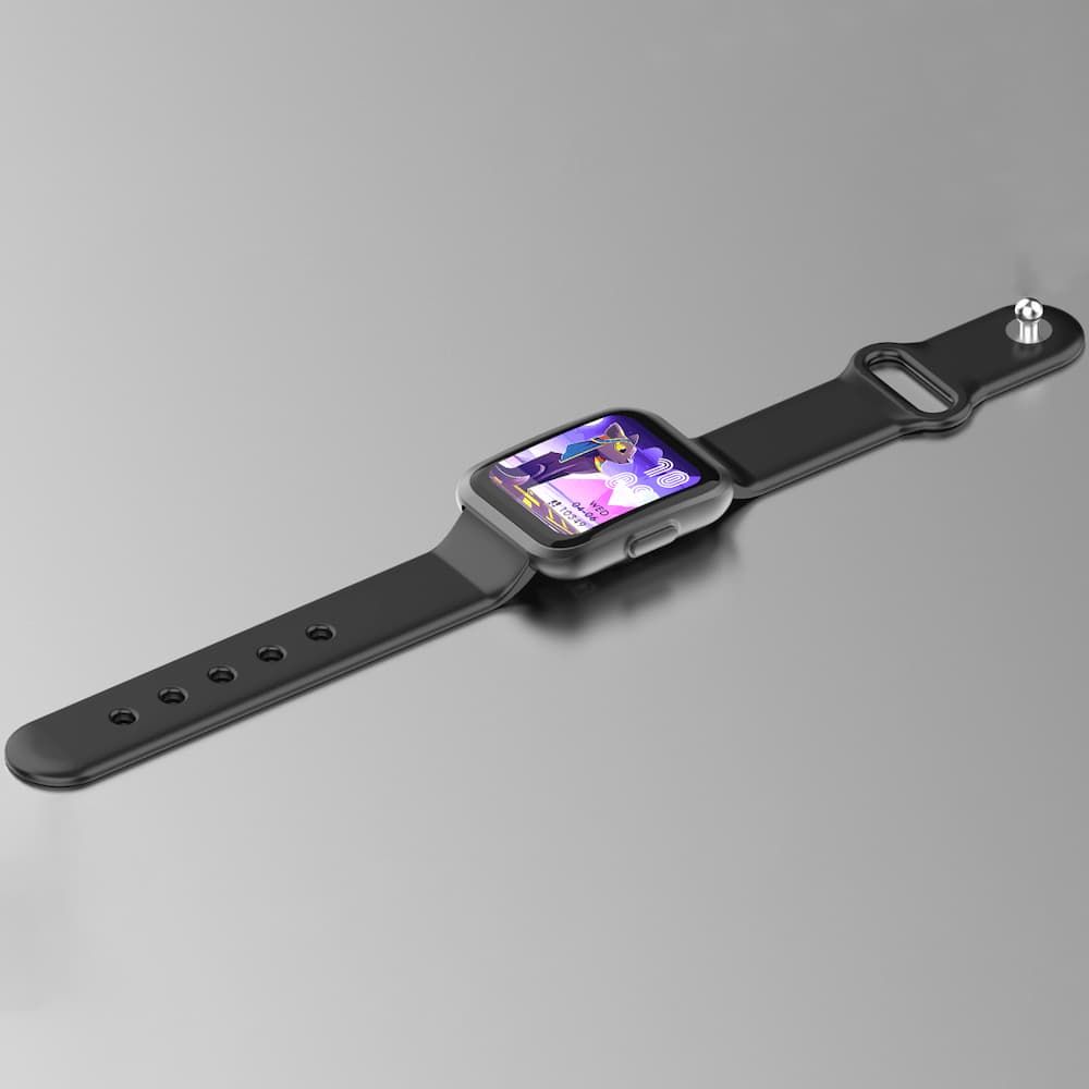
- Wearable Vital Sign Monitors: Including medical-grade smart SpO2 watches, HRV analyzers, portable ECG patches, dynamic blood glucose monitors, and EEG headbands, the design supports real-time collection, processing and local storage of multiple physiological signals, and matches with mobile APP or cloud monitoring platforms to realize remote health management, suitable for home health monitoring and clinical patient follow-up scenarios.
- Surgical Robot Wearable Control Terminals: Suitable for operator wearable control devices for surgical robots and vascular interventional robots, the design adopts 16-layer high-TG board architecture, supports gigabit Ethernet communication and multi-axis motion control real-time response, the signal delay is lower than 1ms, ensuring the synchronization of control actions and robot feedback, and meeting the high reliability requirements of surgical scenarios.
- Implantable Medical Wearables: Including implantable cardiac monitors, implantable nerve stimulators, etc., the design adopts ultra-thin rigid-flex PCB and nano biocoating, the overall thickness of the board can be as low as 0.3mm, which adapts to long-term implantation in the human body, supports low-power wireless data transmission, and the service life of the equipment can reach more than 5 years.
- Wearable Diagnostic Devices: Including portable ultrasound wearable probes, medical endoscope wearable display terminals, etc., the design supports high-speed image signal transmission, anti-interference design suitable for clinical use scenarios, and the signal transmission accuracy can reach 99.99%, ensuring the clarity of diagnostic images.
Key Advantages
- Full-Process Design Service Coverage: Provide one-stop service from requirement docking, schematic design, PCB layout, stackup planning, simulation verification to prototype testing and mass production process docking, reduce cross-party communication costs, ensure the consistency of design schemes and manufacturing processes, and avoid design rework caused by process mismatch.
- Mature Medical Scenario Experience: Have accumulated a large number of verified design solutions for different medical wearable categories, can quickly match mature design frameworks according to product functional requirements, shorten the product development cycle by 30% on average, and reduce trial and error costs in the design process.
- High Customization Flexibility: Support customized design for special requirements such as ultra-low power consumption, IP68 waterproofing, 180-degree repeated flexible bending, and specific communication protocols, adapt to different product form factors including wrist-worn, patch, implantable, head-mounted, and garment-mounted, meeting the differentiated needs of different application scenarios.
- Comprehensive Testing Support: Equipped with full set of testing capabilities covering signal integrity testing, EMC testing, biocompatibility testing, high and low temperature cycle testing, sweat corrosion testing and drop testing, can provide full performance verification before mass production, ensure that products meet clinical use and regulatory requirements, and improve the first-pass rate of mass production.
Contact Information
If you have customized needs for medical wearable PCB design, including functional requirement evaluation, design feasibility analysis, prototype testing consultation, or mass production process docking, you can contact our technical team at any time. We will provide you with targeted design solutions, free pre-project technical evaluation, and full-cycle professional technical support to help your medical wearable products meet regulatory requirements and launch to the market quickly.