Overview
Battery management systems (BMS) are the core control units for all types of rechargeable battery packs, responsible for monitoring cell voltage, temperature, charge/discharge current, state of charge (SOC), and state of health (SOH), while executing protection mechanisms against overcharge, over-discharge, overcurrent, and short circuit. The quality of battery management PCB design directly determines the safety, service life, and energy efficiency of the entire battery system, as well as its ability to operate stably in complex, harsh environments. Common pain points in BMS PCB design include thermal runaway caused by insufficient heat dissipation for high-current paths, signal distortion of sensing and communication interfaces due to crosstalk between high-power and low-voltage signal circuits, and reduced manufacturing yield due to poor design for manufacturability (DFM). Professional battery management PCB design services address these challenges by integrating thermal management, signal integrity optimization, power transmission efficiency improvement, and manufacturability verification into every stage of the design process, delivering reliable, high-performance PCB solutions tailored to specific BMS application scenarios. The end-to-end design process covers schematic design, stack-up planning, component placement, routing optimization, simulation verification, and prototype testing, meeting the performance requirements of BMS systems across all power levels and use cases.
Technical Capabilities
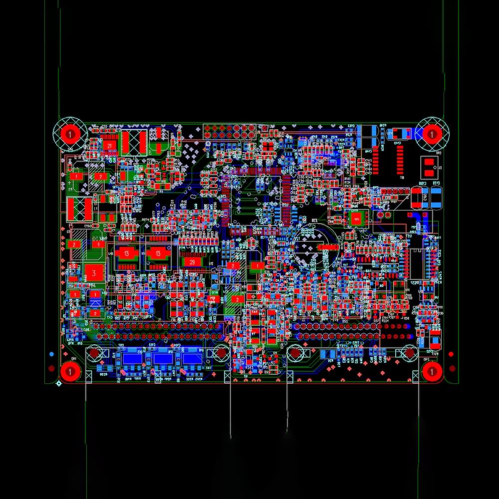
- Custom Stack-up Design: Supports up to 24-layer PCB stack configurations, with options for built-in copper blocks, buried resistance/capacitance layers, buried component layers, and independent ground planes to optimize thermal dissipation and reduce signal interference for high-current BMS systems. Heavy copper configurations up to 12oz are supported for high-current power paths, eliminating voltage drop and localized overheating issues common in high-capacity BMS systems, while buried resistance and capacitance layers reduce the need for discrete components, shrinking the overall PCB form factor by up to 20% for compact applications.
- High-Precision Routing and Component Placement: Achieves minimum line width/space of 2.0/2.0mil, supports component packages as small as 01005 (0.3mm*0.2mm), with placement clearance of ≥3mm from board edges for mark points and top surface components to ensure manufacturing yield and assembly reliability. Minimum 0.5 pitch component placement accuracy is guaranteed, even for dense BMS designs with hundreds of sensing channels, while the 3mm minimum clearance for mark points and edge components ensures compatibility with standard SMT assembly processes, reducing assembly error rates by more than 15% compared to non-standard designs. The design also supports double-sided component placement with device height up to 25mm, adapting to compact BMS form factors for portable and space-constrained applications.
- Signal and Power Integrity Optimization: Delivers ±5% impedance control accuracy for DC/AC power lines and I2C, TDM, PCM communication interfaces, reducing signal attenuation and crosstalk between sensing circuits and power transmission paths. Isolation routing and ground plane segmentation designs are implemented to separate high-voltage power paths from low-voltage sensing and communication circuits, eliminating electromagnetic interference that could lead to inaccurate cell voltage or temperature readings. The design also supports high-voltage isolation structure configuration to prevent short circuits and ensure BMS safety compliance for high-capacity battery packs.
- Special Material and Board Type Adaptation: Supports a wide range of board materials and types including ceramic substrates, metal core substrates, semi-flexible boards, rigid-flex boards, high-resistance carbon oil boards, HDI boards, and high-frequency hybrid boards, adapting to different BMS application requirements for vibration resistance, thermal conductivity, and flexible form factor integration. Ceramic substrate options deliver 5x higher thermal conductivity than standard FR4 materials, making them ideal for high-power BMS systems operating in high-temperature environments, while rigid-flex configurations eliminate the need for connecting cables between BMS control units and battery modules, improving overall system reliability.
- Size and Form Factor Flexibility: Supports conventional PCB sizes up to 600mm450mm, as well as custom unconventional sizes compatible with semi-automatic printing equipment up to 450mm400mm, adapting to BMS designs for battery packs of all capacities from small portable devices to large industrial energy storage systems. Custom outline designs including irregular shapes, cutouts, and edge plating are also supported to match specific battery pack enclosure requirements.
Quality Standards
- Reliability Testing Compliance: All design outputs are validated for thermal cycling performance, vibration resistance, humidity resistance, and high-voltage insulation, ensuring stable operation across industrial-grade temperature ranges from -40°C to +85°C. Simulation tests for thermal dissipation, voltage drop, and signal integrity are conducted during the design stage to identify potential performance issues before prototype production, reducing iteration cycles by up to 30%.
- Manufacturability (DFM) Verification: Designs are pre-validated for manufacturing feasibility, including solder paste printing compatibility, reflow process adaptability, test point coverage, and repair accessibility, reducing prototype iteration cycles and mass production yield loss. DFM checks cover minimum line width/space, via size, component clearance, and solder mask alignment, ensuring designs are compatible with standard mass production processes without requiring costly equipment upgrades or process adjustments.
- Functional Safety Alignment: Designs comply with relevant functional safety standards for battery systems, including overcharge/discharge protection circuit verification, temperature sensing loop redundancy, and communication interface fault tolerance, minimizing safety risks for battery packs. All protection circuit paths are designed with redundant routing to ensure protection functions remain operational even if a single routing path is damaged, meeting the functional safety requirements for automotive and industrial BMS applications.
Applications
- Consumer Electronics BMS: For lithium-ion battery packs in smartphones, laptops, power banks, electric scooters, and wearable devices, supporting compact form factors, low power consumption, and high charge/discharge efficiency.
- Electric Vehicle (EV) BMS: For power battery packs in passenger EVs, commercial electric vehicles, and electric two-wheelers, supporting high-current transmission, wide temperature range operation, and CAN bus communication stability.
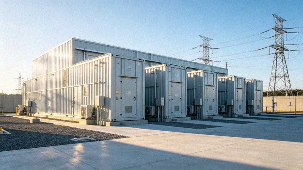
- Energy Storage System (ESS) BMS: For residential and industrial solar energy storage, grid-scale energy storage, and backup power systems, supporting multi-string battery monitoring, high-voltage isolation, and long-term operational reliability.
- Industrial Equipment BMS: For battery-powered industrial robots, AGVs, medical portable devices, and telecom backup power supplies, supporting vibration resistance, high EMI immunity, and compliance with industrial quality standards.
- Aerospace and Defense BMS: For battery systems in drones, satellite power supplies, and military portable equipment, supporting extreme temperature tolerance, radiation resistance, and high reliability in harsh operating environments.
Key Advantages
- End-to-End Design Support: Covers the full design lifecycle from schematic drawing, stack planning, placement and routing optimization, simulation verification, to prototype testing, eliminating cross-vendor communication gaps and ensuring design consistency. Technical teams work closely with clients to align design outputs with specific BMS performance, cost, and timeline requirements.
- Customization for Special Requirements: Supports custom configurations for buried components, embedded copper blocks, ceramic substrates, and rigid-flex structures, addressing unique BMS design requirements for high power, compact size, and flexible installation. Custom material and process combinations are available for niche use cases with extreme environmental performance requirements.
- Cost and Time Optimization: DFM verification is integrated at every design stage, reducing prototype iteration times by up to 30% and lowering mass production costs by avoiding unnecessary high-end material overuse and manufacturing defects. Design teams also balance performance requirements with manufacturing cost to deliver the most cost-effective solutions without compromising reliability.
- Scalable Design Solutions: Adaptable to both small-batch prototype verification needs and large-scale mass production design requirements, with standardized design processes that ensure consistent performance across production batches. Design files are fully optimized for mass production, eliminating rework requirements when scaling from prototype to high-volume manufacturing.
Contact Information
If you have customized battery management PCB design requirements, or need technical consulting for BMS circuit layout, thermal management, signal integrity optimization, or manufacturability verification, please reach out to our technical team. We will provide you with targeted design solutions, free pre-design feasibility evaluation, and professional technical support to help you bring high-reliability BMS products to market efficiently.