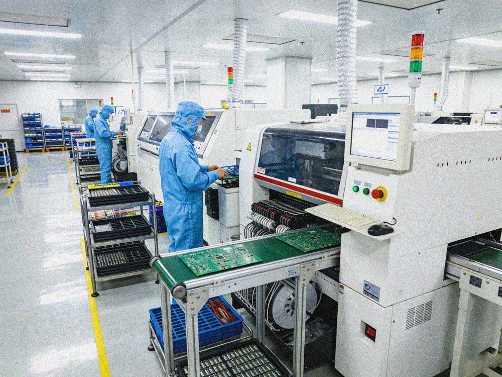
Overview
The rapid development of intelligent connected vehicles and autonomous driving technology has led to a sharp increase in the number of electronic components integrated into automotive systems, placing extremely high demands on the size, performance, and reliability of automotive PCBs. Automotive PCB high density design is a core technical solution to address these needs, enabling the integration of high-performance processing chips, sensor interfaces, power modules, and communication units in limited on-board space, while ensuring stable signal transmission, efficient heat dissipation, and long-term reliable operation in harsh automotive operating environments. Common challenges in automotive PCB design include signal crosstalk caused by high-density routing, impedance mismatch leading to high-speed signal distortion, thermal buildup from high-power modules, and reduced reliability under long-term vibration, temperature fluctuation, and humidity. A standardized high density design process covers full-chain optimization from material selection, stack architecture planning, placement and routing adjustment, to simulation and verification, effectively solving the above pain points, and meeting the strict performance and compliance requirements of the automotive electronics industry.
Technical Capabilities
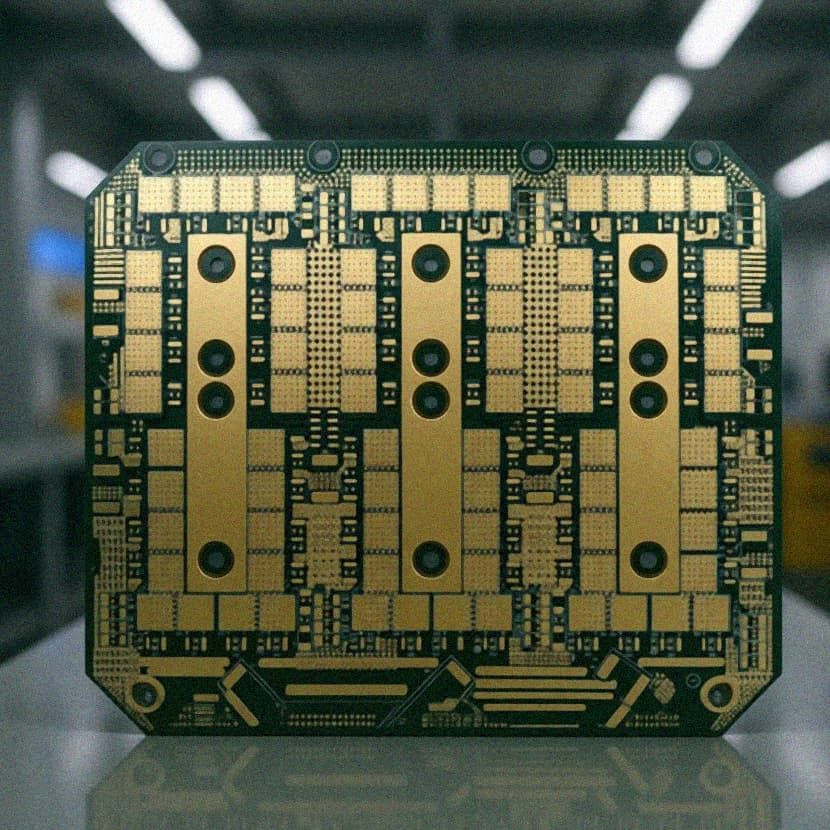
- HDI and Micro-Via Design Support: Supports 1+N+1, 2+N+2 and other multi-stage HDI stack configurations, with micro-vias as small as 0.06mm and line width/space down to 2.0/2.0mil, enabling compact routing for high-component density automotive boards, accommodating large numbers of sensors, processing units, and interface modules in limited installation space, reducing overall board size by up to 30% compared to conventional designs.
- High-Speed Multi-Layer Design Expertise: Supports up to 30+ layer high-speed PCB stack designs, with configurable independent ground planes to shield cross-layer signal interference, adapting to high-speed I/O transmission requirements of up to 750Gbps, meeting the low-latency, high-fidelity signal transmission needs of automotive AI computing units with peak computing power of 32TOPS and above.
- Special Material and Structure Adaptation: Supports design of buried copper block, buried ceramic, heavy copper, rigid-flex, and high-frequency hybrid boards, optimizing thermal dissipation by up to 40% compared to standard FR4 designs, adapting to high-power automotive modules such as motor drives, charging inverters, and power supply units. Rigid-flex design solutions also eliminate the need for separate connector wiring, improving vibration resistance for cockpit and chassis-mounted hardware.
- Precision Impedance Control: Achieves ±5% impedance control accuracy for 90Ω, 100Ω, and other common automotive signal impedance requirements, reducing signal reflection, attenuation, and crosstalk, ensuring stable transmission of differential signals, high-bandwidth memory signals, and 77G radar RF signals without data loss or delay.
- Embedded Component Design Capability: Supports design of buried resistance, buried capacitance, and buried component boards, reducing surface mount space occupancy by up to 25%, further improving board density and reducing the risk of component falling off under long-term vibration, significantly improving the environmental adaptability of on-board hardware.
Quality Standards
- Automotive Industry Compliance: All design processes follow IATF 16949 automotive quality management system requirements, with design verification processes aligned to AEC-Q200 component reliability standards, ensuring products meet automotive grade durability requirements for 10+ year service life.
- Reliability Testing Coverage: Designs are validated through a full suite of reliability tests before mass production, including -40°C to +85°C wide temperature cycle testing, 10-2000Hz vibration and 1500G shock testing, CISPR 25 EMC compliance testing, and 1000-hour thermal cycling testing, ensuring stable operation under extreme automotive operating conditions such as high humidity, salt spray, and long-term road vibration.
- Manufacturability Optimization: All designs undergo strict DFM (Design for Manufacturing) and DFT (Design for Testing) validation before entering production, identifying and resolving potential manufacturing defects in the design stage, ensuring over 95% manufacturing yield for high-density boards, reducing production costs, and shortening product launch cycles for automotive electronics customers.
Applications
Automotive PCB high density design solutions are widely applicable to a full range of automotive electronic scenarios, including but not limited to:
- Autonomous driving domain controllers and ADAS core processing units
- 77G vehicle-mounted millimeter wave radar, LiDAR and other perception hardware
- Smart cockpit core boards, intelligent central control displays, and in-vehicle navigation systems
- Vehicle motor drive modules, DC/DC power modules, and charging inverter integrated units
- Intelligent rearview mirrors, in-vehicle camera acquisition boards, and signal filtering modules
- High-speed backplanes for in-vehicle communication networks and automotive IC substrates
- Semi-flexible boards for compact cabin installation and mini-LED backlight display boards
Key Advantages
- Space and Performance Balance: High density routing reduces overall board size while maintaining high signal transmission performance and heat dissipation capacity, supporting the miniaturization and lightweight trend of automotive electronic components, which helps reduce overall vehicle energy consumption.
- Customizable Design for Specific Scenarios: Solutions can be fully customized according to application requirements, including high-frequency PTFE material configurations for radar modules, 10oz+ heavy copper configurations for power modules, and rigid-flex configurations for compact cockpit installations, adapting to the differentiated needs of different automotive subsystems.
- Full Lifecycle Support: Covers the entire design process from schematic verification, stack planning, placement and routing optimization, signal integrity simulation verification, to prototype testing, supporting R&D verification, small batch trial production and mass production transition requirements, reducing cross-stage communication and iteration costs for customers by over 40%.
- High Compatibility with Mainstream Automotive Chip Platforms: Design solutions are pre-adapted to mainstream automotive processing chip platforms including NXP I.MX series, Renesas TW series, and Xilinx Zynq series, reducing design adaptation time and accelerating product R&D progress by 30% on average.
Contact Information
If you have automotive PCB high density design needs, or require technical evaluation and customization support for automotive PCB projects, please reach out to our professional technical team. We will provide you with targeted design solutions, free DFM evaluation, and professional technical consulting services to support the smooth launch of your automotive electronic products.