Overview
AI signal integrity PCB design is a core technical link to ensure the stable operation of high-performance AI hardware, especially for edge autonomous computing devices, data center AI acceleration modules, and high-computing-power industrial AI equipment. The concentrated deployment of high-density computing units, high-bandwidth memory interfaces, and 750Gbps+ high-speed I/O interfaces in AI hardware leads to extremely high requirements for signal transmission quality. Common problems including signal attenuation, crosstalk, impedance misalignment, reflection, and transmission delay can directly reduce AI computing performance, cause data transmission errors, and even lead to system-level downtime in severe cases. Our AI signal integrity optimized PCB design services cover the entire process from schematic design review, stack structure planning, component placement and routing optimization, to pre-production simulation and post-production testing verification, fully meeting the design needs of various high-end AI hardware with different computing power levels and application scenarios.
Technical Capabilities
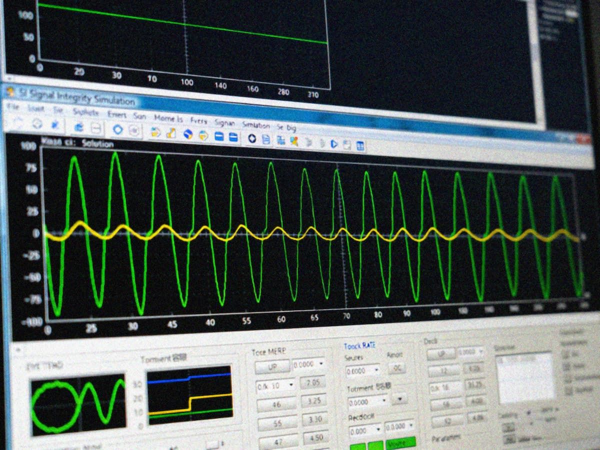
- Pre-Production Signal Integrity Simulation: We adopt industry-leading high-speed PCB design signal integrity analysis tools built on mainstream EDA platforms, with more than 400 embedded application functions, to realize full-link simulation and risk prediction of signal reflection, crosstalk, transmission delay, impedance mismatch, and electromagnetic interference before the prototyping stage. This can effectively identify potential design flaws in advance, reduce post-production iteration costs by more than 60%, and shorten the overall product R&D cycle.
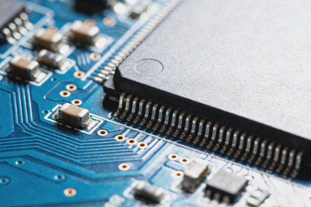
- Customized Stack Architecture Design: We support 4 to 20+ layer PCB stack design solutions, with configurable multi-layer independent ground planes, power plane partitioning, and interference shielding layer settings, which can effectively isolate interference between different signal layers, adapt to high-density routing requirements of high-performance AI hardware with peak computing power up to 200TOPS, and balance design performance and manufacturing cost.
- High-Precision Impedance Control: We achieve ±5% industry-leading impedance control accuracy for 50Ω single-ended signals, 90Ω and 100Ω differential signals, which perfectly adapts to the transmission requirements of mainstream high-speed interfaces including MIPI CSI, DDR5, HBM3, PCIe 6.0, and 10G/40G/100G Ethernet, minimizing signal reflection loss and transmission distortion, and ensuring 99.99%+ data transmission accuracy.
- High-Speed Signal Adaptation: Our design solutions support up to 750Gbps high-speed I/O performance, 40Gbps D-PHY 1.2, 62Gbps C-PHY 1.1, and 112Gbps SerDes transmission rates, fully meeting the low-latency, high-fidelity signal transmission requirements for large-scale data interaction between AI computing units, memory modules, and peripheral expansion interfaces, avoiding data bottlenecks in high-computing-power AI operation processes.
- Multi-Parameter Routing Optimization: We implement targeted routing rules for different signal types, including equal-length matching for high-speed differential pairs, isolated routing for sensitive clock and analog signals, 3W spacing control for adjacent signal lines, and via stub length reduction, which further eliminates crosstalk between adjacent lines and signal delay deviation caused by inconsistent transmission paths.
- Full-Cycle Verification Support: We provide end-to-end verification services covering signal integrity testing, power integrity testing, EMC/EMI testing, and environmental reliability testing, which can locate and solve remaining signal problems in the prototype stage, ensuring products meet long-term stable operation requirements under complex working conditions.
Quality Standards
- Design Compliance Standards: All design processes strictly follow IPC-2221, IPC-2223, and other international general PCB design specifications, and design output documents are fully compatible with mainstream PCB manufacturing process requirements, ensuring a design manufacturability rate of more than 99%, and avoiding design flaws that lead to mass production rejection.
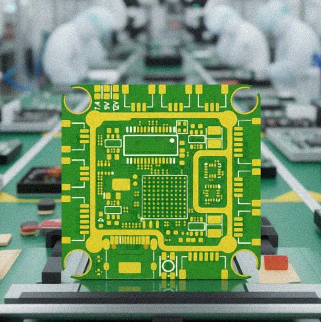
- Manufacturing Process Adaptability: Our design solutions support a full range of advanced PCB manufacturing processes, including HDI boards, rigid-flex boards, high-frequency hybrid boards, heavy copper boards, buried resistance and buried capacitance boards, embedded component boards, and high-speed backplanes, with support for line width/line spacing as small as 2.0/2.0mil, micro-via diameter down to 0.06mm, fully meeting the high-density integration needs of miniaturized AI hardware.
- Reliability Testing Specifications: All verification items are carried out in accordance with ISO/IEC 17025 accredited testing specifications, covering high and low temperature cycle testing, vibration and shock testing, salt spray corrosion testing, and long-term aging testing, ensuring that products can operate stably in industrial-grade temperature ranges from -40℃ to +85℃, and adapt to harsh application scenarios such as industrial sites, outdoor monitoring, and vehicle-mounted environments.
- Material Selection Specifications: We support the matching of various high-frequency, low-loss substrate materials including Rogers series, TU-872, MEGTRON 6/7, etc., adjusting substrate parameters such as dielectric constant and loss tangent according to signal transmission frequency and power consumption requirements, further reducing signal attenuation in high-frequency and high-speed transmission scenarios.
Applications
AI signal integrity PCB design solutions are widely applicable to various AI-driven hardware scenarios, including but not limited to:
- Edge AI computing nodes and 5G edge gateway equipment for smart cities
- Autonomous driving domain controllers, in-vehicle AI computing platforms, and smart cockpit core control units
- Industrial AI inspection robots, intelligent logistics AGV control units, and industrial automation intelligent control terminals
- Medical AI assisted diagnostic equipment, biological signal analysis devices, and medical imaging processing systems
- Data center AI acceleration cards, high-performance computing servers, and cloud AI processing modules
- Smart retail interactive terminals, computer vision recognition devices, and face recognition access control systems
- Agricultural intelligent monitoring terminals, agricultural AI pest and disease analysis equipment, and smart agricultural control systems
- Consumer-grade AI edge devices including smart cameras, voice interaction terminals, and home intelligent control hosts
Key Advantages
- End-to-End Service Coverage: We provide one-stop services covering schematic design review, PCB layout optimization, prototype manufacturing, PCBA assembly, to final testing and verification, which reduces cross-stage communication costs and information asymmetry, shortens the overall product R&D cycle by 30% on average, and ensures that design solutions are fully feasible for mass production.
- Mature Project Implementation Experience: We have completed hundreds of signal integrity design projects for high-performance AI hardware including AI evaluation boards, edge computing modules, and high-speed backplanes, with verified mature solutions that can effectively solve common industry pain points such as high-speed signal transmission instability, high manufacturing rejection rates, and poor environmental adaptability.
- Customized Solution Support: We adjust design strategies and technical parameters according to different application scenarios, performance indicators, and cost budgets, fully balancing product performance, manufacturability, and production cost, which is suitable for different demand stages including R&D verification, small batch trial production, and large-scale mass production.
- Continuous Technical Iteration: We continuously update our design simulation libraries, routing rules, and optimization schemes according to the latest AI hardware interface standards and manufacturing process developments, currently supporting the latest generation of HBM3, PCIe 6.0, and 112G SerDes interface design requirements, which can adapt to the rapid iterative needs of next-generation high-computing-power AI hardware.
Contact Information
If you have any needs related to AI signal integrity PCB design, including technical consultation, design scheme evaluation, customized service inquiry, or manufacturing feasibility assessment, please contact our professional technical team through the official website consultation channel, service hotline, or business email. We will provide you with targeted design solutions, free pre-sales technical evaluation, and full-cycle technical support according to your specific project requirements, helping you quickly complete product R&D and mass production landing.