Overview
The rapid development of high-performance AI hardware, including data center GPU accelerators, edge computing units, and autonomous driving perception systems, has brought unprecedented challenges to PCB design. These systems are usually integrated with high-density computing chips, 100G+ high-speed I/O interfaces, and high-bandwidth memory modules, leading to concentrated high-speed signal transmission and complex power distribution requirements. Without targeted design optimization, common issues such as signal attenuation, crosstalk, impedance mismatch, and electromagnetic interference (EMI) will directly reduce AI computing efficiency, cause data transmission errors, and even lead to hardware failure.
AI high speed PCB design is a specialized design service tailored for AI hardware scenarios, covering the entire process from schematic review, stack architecture planning, component placement and routing optimization, to performance testing and verification. The design focuses on ensuring signal integrity, power integrity, and thermal stability of high-speed transmission links, while complying with manufacturing feasibility requirements, to support stable operation of AI hardware with peak computing power ranging from 16TOPS to 128TOPS.
Technical Capabilities
- Multi-layer stack design optimization: Supports up to 32-layer PCB stack configuration, with optional dedicated independent ground planes, high-frequency hybrid substrates, ceramic-filled laminates, and other material combinations, effectively shielding cross-layer signal interference, adapting to high-density routing requirements of high compute density AI hardware. The stack design can be customized according to signal rate, power distribution requirements, and board size constraints to balance performance and manufacturing cost.
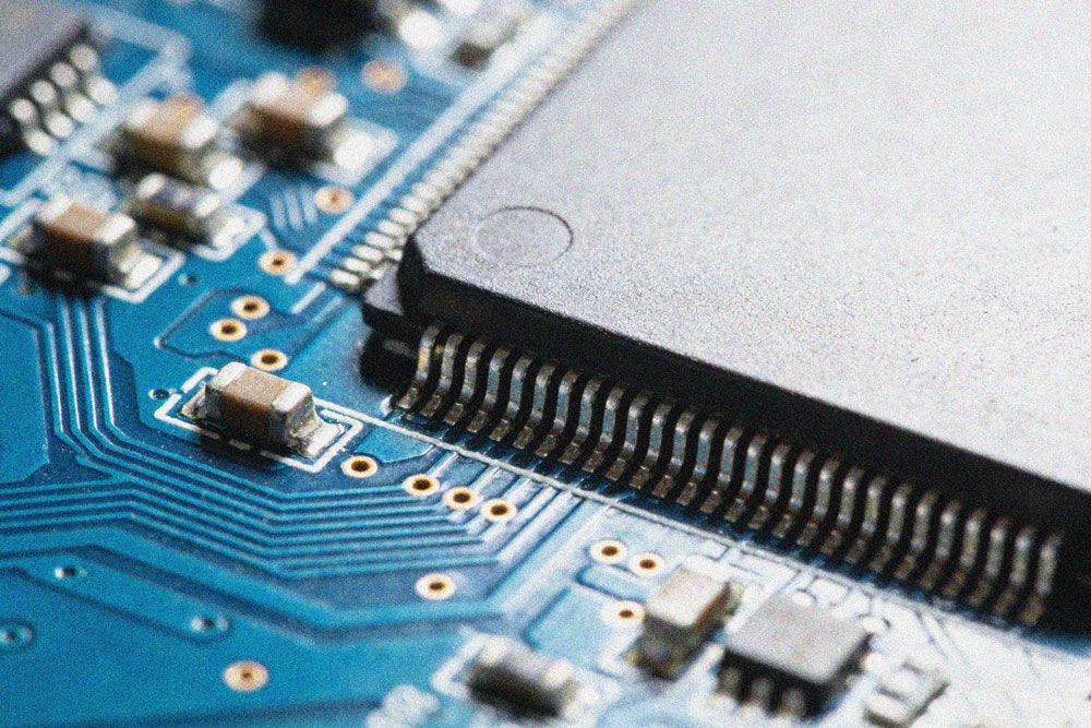
- Precise impedance control capability: Achieves ±5% impedance control accuracy for 90Ω differential pairs, 100Ω high-speed transmission lines, and 50Ω single-ended signals, reducing signal reflection loss and inter-symbol interference. It is fully compatible with transmission requirements of high-speed differential signals, MIPI CSI/DSI, DDR5, and high-bandwidth memory (HBM) interfaces, ensuring error-free data transmission between computing chips and peripheral modules.
- High-speed signal adaptation support: Supports up to 800Gbps high-speed I/O transmission rates, compatible with PCIe 6.0, CXL 3.0, 112G SerDes, and other mainstream high-speed interface protocols, meeting low-latency, high-fidelity data transmission requirements of AI hardware with up to 128TOPS peak computing power. The design includes targeted optimization for high-speed backplane links, reducing insertion loss and return loss across the entire transmission path.
- Special process compatibility: Supports design of multiple special PCB types for AI scenarios, including HDI boards, rigid-flex boards, heavy copper boards, high-frequency hybrid boards, buried resistance/capacitance boards, buried component boards, buried copper block boards, ceramic boards, and semi-flexible boards, adapting to diverse form factor, heat dissipation, and performance requirements of AI hardware for different application scenarios.
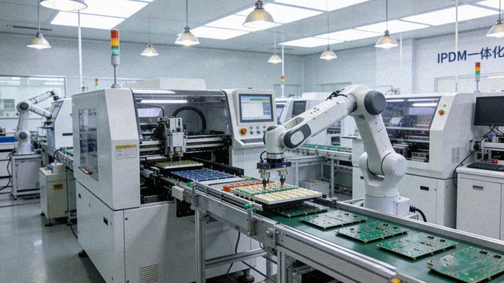
- Full-process verification service: Provides end-to-end verification services including signal integrity (SI) simulation and testing, power integrity (PI) analysis, EMC/EMI testing, thermal simulation, and high/low temperature reliability testing, identifying potential design risks before manufacturing, reducing prototype iteration times and overall project development cycles.
Quality Standards
All AI high speed PCB design processes strictly follow international industry specifications to ensure design reliability and manufacturing feasibility. The design complies with IPC-2221 high-speed PCB design specifications, IPC-9701 performance test standards, and RoHS, REACH environmental protection requirements.
Before finalizing design files, mandatory DFM (design for manufacturing), DFA (design for assembly), and DFT (design for testing) checks are carried out to ensure design solutions are compatible with mass production processes, reducing rework costs and shortening production lead times. For prototype and mass production runs, 100% impedance testing, continuity testing, and insulation resistance testing are required to ensure that the produced boards fully meet design specifications.
For industrial-grade and automotive-grade AI hardware, the design meets wide temperature operation requirements from -40℃ to +85℃, and complies with vibration and shock resistance standards for harsh operating environments, ensuring long-term stable operation of products in complex application scenarios.
Applications
AI high speed PCB design solutions are widely applicable to various AI-driven hardware scenarios, including but not limited to:
- Data center AI accelerator cards, GPU computing boards, and AI server motherboards
- Edge AI computing nodes for smart cities, industrial IoT, and energy monitoring systems
- Autonomous driving domain controllers and in-vehicle AI computing platforms
- Intelligent medical diagnostic equipment and medical AI inference units
- AI-powered industrial inspection robots and logistics autonomous transport vehicles
- High-resolution intelligent monitoring terminals and facial recognition access control devices
- Mini-LED backlight display control boards for AI interactive terminals and smart cockpit displays
- AI voice interaction terminals and natural language processing edge devices
Key Advantages
- Performance and cost balanced design: All design solutions are optimized based on actual application requirements, balancing performance, manufacturing cost, and lead time. Compared with non-specialized design services, it can reduce overall project costs by 20% to 30% while meeting performance indicators, and shorten product time to market by up to 40%.
- High-density routing capability: Supports micro-vias as small as 0.06mm, line width/line spacing as low as 2.0/2.0mil, enabling compact layout of high-density AI chips and peripheral components, reducing overall board size by up to 25% while maintaining signal integrity, adapting to the miniaturization demand of portable and embedded AI hardware.
- Customized solution support: Tailors stack design, material selection, routing strategy, and testing scheme according to specific application scenarios, supporting diverse requirements from prototype verification, small-batch trial production to large-scale mass production. It can also provide targeted optimization for special requirements such as heat dissipation, anti-interference, and wide temperature operation.
- Full lifecycle technical support: Covers end-to-end services from schematic review, PCB layout, prototype fabrication, PCBA assembly to performance testing, supporting iterative adjustment during product development, and providing technical guidance for subsequent mass production and quality control.
Contact Information
If you have AI high speed PCB design requirements, or need technical consultation related to high-speed signal transmission, impedance control, design for manufacturing, or process compatibility, please reach out to our technical support team. We will provide you with customized design solutions, free pre-design feasibility evaluation, and professional technical guidance to support the successful development and mass production of your AI hardware products.