Overview
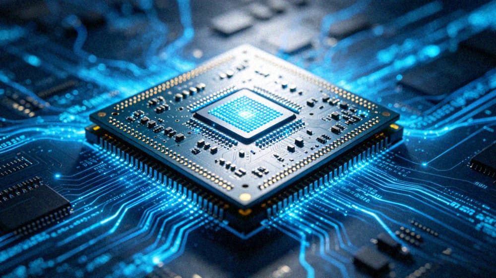
AI hardware PCB design is the core foundation for ensuring stable operation and full performance release of high-computing-power AI systems. As modern AI products continue to improve in computing power, with single-chip computing power reaching 16TOPS and even higher, the dense layout of GPU, FPGA, DSP, and ARM core platforms, paired with high-bandwidth memory interfaces and 750Gbps high-speed I/O ports, puts forward extremely high requirements for PCB routing density, signal integrity, thermal management, and manufacturing feasibility. Poor design will directly lead to problems such as signal attenuation, crosstalk, impedance mismatch, and thermal throttling, reducing AI computing efficiency, increasing data transmission error rates, and even leading to product failure in severe cases.
Our AI hardware PCB design services cover the entire chain from demand demonstration, schematic design, stack planning, placement and routing optimization, DFM review, prototype fabrication to mass production guidance, targeting the core pain points of AI hardware development, providing design solutions that balance performance, reliability and manufacturing cost, and meeting the design needs of various AI products from edge terminals to data center high-performance computing equipment.
Technical Capabilities
- Multi-Platform Design Adaptation: Supports ARM, DSP, FPGA, and GPU core platform designs, compatible with high-computing-power SoC chips up to 16TOPS and above, matching AI compilation tools and SDK suites to accelerate product verification and iteration, cutting the time from design to functional verification by 35% on average.
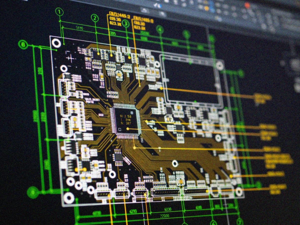
- High-Speed & High-Density Routing Optimization: Supports high-layer PCB designs up to 40+ layers, with micro-vias as small as 0.06mm and line width/space down to 2.0/2.0mil, adapting to high-density component placement of HDI boards, buried component boards, high-speed backplanes, and rigid-flex board designs, suitable for miniaturized AI terminal and high-density computing card scenarios.
- Thermal Management Optimization: Targeted thermal design for high-power AI hardware, supporting high-heat-dissipation PCB structures including buried copper blocks, ceramic substrates, and thick copper layers, reducing thermal resistance by up to 30% to avoid performance throttling caused by overheating of computing units, and ensuring stable operation under long-term full-load operation conditions.
- Signal Integrity Guarantee: Achieves ±5% impedance control accuracy for 90Ω/100Ω differential signals, supports high-speed I/O transmission up to 750Gbps, and provides pre-simulation and post-testing of signal crosstalk, attenuation, and delay to ensure stable transmission of high-bandwidth memory and interface data, reducing data transmission error rate to less than 10-12.
- Full-Stack Design & Manufacturing Integration: Covers schematic optimization, BOM optimization, component selection, stack planning, placement and routing, prototype fabrication, testing, and mass production support, eliminating cross-stage communication gaps and improving development efficiency by 40% on average, while reducing the risk of design rework caused by manufacturing incompatibility.
Quality Standards
- All design processes strictly comply with IPC-A-610, IPC-2221, RoHS, and CE international industry standards, meeting the reliability requirements of industrial, commercial, and automotive-grade application scenarios, and adapting to harsh working environments such as high humidity, high salt spray, and wide temperature fluctuations.
- Strict three-level design review mechanism: each design undergoes independent review of DFM (design for manufacturing), DFT (design for testing), and DFR (design for reliability) before entering the production stage, effectively reducing prototype iteration cycles by 50% on average, and lowering the probability of design rework to less than 3%.
- Full coverage of reliability testing links: each finished design supports optional verification services including signal integrity testing, EMC/EMI testing, high and low temperature cycle testing, vibration and shock testing, and thermal cycling testing, ensuring products operate stably in -40℃ to +85℃ industrial-grade temperature environments, with an average service life of 10+ years for static application scenarios.
- Material compliance guarantee: All selected PCB substrates meet UL 94 V-0 flame retardant standards, with optional high-frequency, high-Tg, low-DK materials to adapt to the transmission requirements of high-frequency AI communication and perception modules, and meet the lead-free and halogen-free environmental requirements of different regional markets.
Applications
AI hardware PCB design solutions can be widely adapted to various AI-driven product scenarios, including but not limited to:
- High-Performance Computing Hardware: Including GPU computing cards, FPGA acceleration boards, edge AI core boards, high-speed backplanes for data centers, and AI server motherboard designs.
- Intelligent Robotics Systems: Covering industrial robot main control boards, collaborative robot drive boards, service robot perception interface boards, and agricultural autonomous navigation robot control boards.
- AIoT Intelligent Terminals: Including smart home main control boards, intelligent environmental monitoring terminals, industrial edge computing nodes, 5G AI communication modules, and optical module carrier boards.
- Industrial AI Equipment: Including ATE equipment test boards, power control boards for new energy systems, intelligent industrial inspection equipment motherboards, and machine vision processing board designs.
- Automotive AI Hardware: Adapting to autonomous driving domain controllers, smart cockpit core control units, in-vehicle multi-sensor perception interface boards, and vehicle edge computing platform designs.
Key Advantages
- Customized Scheme Matching: Provides targeted design solutions based on product application scenarios, computing power requirements, and cost constraints, balancing performance, manufacturing feasibility, and production cost to reduce overall BOM cost by 15% to 25% on average without sacrificing product performance.
- Mature Technology Accumulation: Has rich design experience in high-speed mixed signal, rigid-flex board, buried component, high-frequency mixed pressure, and high heat dissipation PCB types, effectively solving common pain points in AI hardware design including high-speed signal loss, power supply noise, and thermal concentration.
- Full-Cycle Technical Support: Provides technical consultation from the early product planning stage, including scheme demonstration, component selection, development environment construction, and post-production debugging support, accompanying the entire product lifecycle from prototype verification to mass production.
- Flexible Production Adaptation: Supports prototype proofing, small-batch trial production, and large-scale mass production demands, with a minimum order quantity of 1 piece for prototype verification, and a lead time of 3 to 7 days for fast prototype delivery to meet the fast iteration requirements of AI product R&D.
Contact Information
If you have any customized demands for AI hardware PCB design, including scheme consultation, design optimization, or prototype fabrication requirements, you can contact our professional technical team at any time. We will provide you with free pre-sales technical evaluation, customized design schemes, and full-process technical support to help your AI product go to market quickly and efficiently.