Overview
High-density interconnect (HDI) PCBs are core components for modern miniaturized, high-performance electronic devices, enabling finer line widths, higher component density, and more efficient signal transmission compared to traditional multilayer PCBs. As electronic products continue to trend toward smaller form factors, higher computing power, and lower power consumption, HDI PCB manufacturing requires highly precise production processes, advanced material compatibility, and strict quality control to address core challenges including signal integrity degradation, heat dissipation optimization, and blind/buried via reliability. Professional HDI PCB manufacturer services support custom design and production of HDI boards for diverse application scenarios, covering both rapid prototyping for product development and large-scale mass production for commercial deployment, ensuring consistent performance and reliability across all project stages.
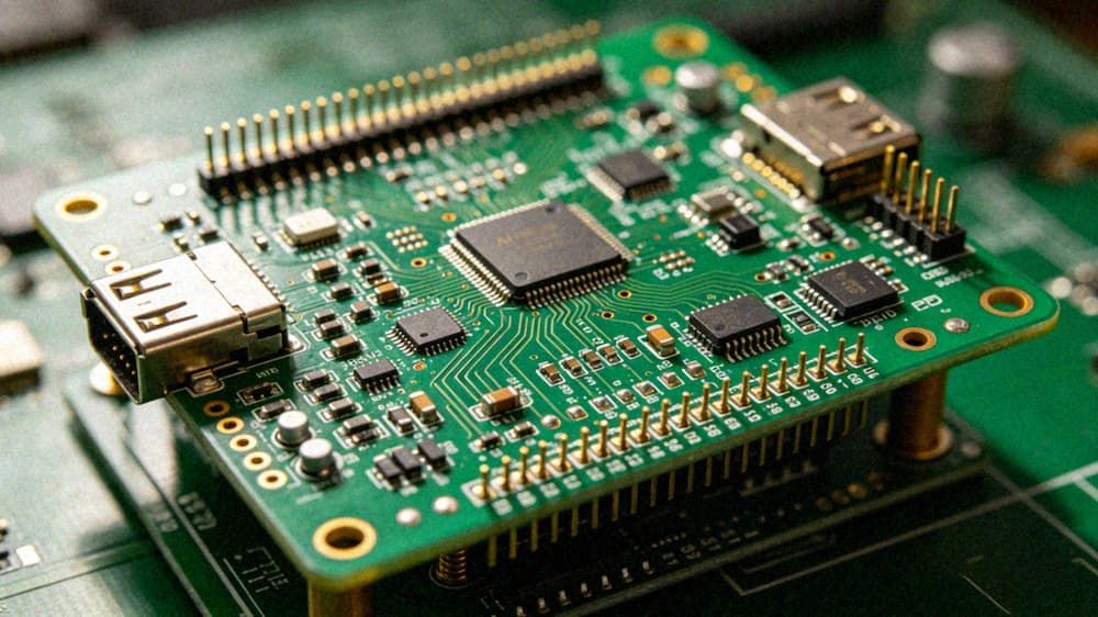
Technical Capabilities
- Layer Count and HDI Type Support: Offers prototyping support for up to 30-layer anylayer HDI boards, and mass production support for up to 26-layer 4-step HDI boards, adapting to diverse project requirements from proof-of-concept to large-scale deployment. Supports both mechanical blind buried via HDI and laser micro-via HDI processes to meet different density and cost requirements.
- High-Speed Signal Compatibility: Supports maximum signal transmission rates of 112Gbps for prototyping projects and 25Gbps for mass-produced HDI boards, meeting the low-latency, low-loss signal transmission needs of high-performance electronic systems including high-speed optical modules, edge computing nodes, and communication infrastructure.
- High-Precision Manufacturing Process: Achieves minimum component pitch accuracy of 0.5mm, supports surface mount for ultra-small components including 01005 packages (0.3mm x 0.2mm), with double-sided component height support up to 25mm to accommodate high-density component placement for complex system designs.
- Flexible Board Size Support: Accommodates custom HDI board sizes up to 550mm x 900mm for prototyping and 550mm x 620mm for mass production, with support for unconventional form factors compatible with semi-automatic and fully automatic assembly processes, adapting to unique product form factor requirements.
- Cross-Material Integration Capabilities: Supports HDI board manufacturing with a wide range of substrate materials including FR4, high-frequency hybrid substrates, PTFE, rigid-flex material combinations, and metal core substrates, adapting to application scenarios with special requirements for heat resistance, signal transmission, and mechanical flexibility.
Quality Standards
All HDI PCB manufacturing processes adhere to global industry standards and undergo multi-stage quality verification to ensure consistent performance and reliability. Processes comply with IPC-A-600 and IPC-6012 standards for HDI board acceptability, with additional compliance certifications available for industry-specific applications including automotive, medical, and industrial electronics. All finished HDI boards undergo a series of rigorous tests before delivery, including:
- Impedance accuracy testing with tolerance control as low as ±10% to ensure stable high-speed signal transmission
- X-Ray non-destructive inspection of blind and buried vias to verify connectivity and eliminate via voiding defects
- Thermal cycling testing between -40°C and +85°C to validate reliability in extreme operating environments
- Signal integrity testing to measure insertion loss, crosstalk, and return loss for high-speed board designs
- Solderability testing and surface finish verification to ensure compatibility with downstream assembly processes Testing facilities hold ISO/IEC 17025 accreditation, with test reports recognized globally for regulatory compliance and product qualification purposes.
Applications
HDI PCB manufacturing solutions are widely applicable across all high-performance electronic industry sectors, including:
- Consumer Electronics: Smartphones, wearable devices, mini LED backlight displays, tablets, portable gaming devices, and wireless earbuds, supporting ultra-compact form factors and low-power high-speed signal transmission.
- Communication Electronics: 5G base station RF components, high-speed optical modules, network switches, Wi-Fi 6/7 routers, and satellite communication terminals, meeting high-bandwidth low-latency signal transmission requirements.
- Automotive Electronics: Advanced driver assistance systems (ADAS), smart cockpit core controllers, autonomous driving domain controllers, in-vehicle infotainment systems, and battery management systems for electric vehicles, with compliance to automotive industry reliability standards.
- Industrial Electronics: Industrial edge computing nodes, IoT gateways, industrial control systems, factory automation sensors, and robotics control boards, supporting stable operation in harsh industrial environments with wide temperature ranges and high vibration.
- Medical Electronics: Portable diagnostic devices, patient monitoring systems, implantable medical equipment, and medical imaging processing units, with compliance to medical industry safety and biocompatibility standards.
- Aerospace and Defense: Compact avionics equipment, satellite communication modules, drone control systems, and military communication devices, with high shock and vibration resistance and extreme temperature adaptability.
Key Advantages
- End-to-End Production Support: Covers full lifecycle support from rapid prototyping, small-batch trial production to large-scale mass production, eliminating the need for cross-supplier handover and reducing project lead times and compatibility risks between design, prototyping, and mass production stages.
- Customized Process Adjustment: Offers tailored material selection, stack-up design, and process optimization based on application-specific requirements for signal speed, environmental adaptability, and form factor, ensuring optimal performance at the lowest possible manufacturing cost, without unnecessary over-engineering.
- High Yield Rate Guarantee: Leverages advanced production equipment including high-precision laser drilling systems, LDI laser direct imaging, and automated optical inspection (AOI) to achieve industry-leading yield rates for complex multi-step and anylayer HDI boards, reducing overall production costs and shortening delivery times for customers.
- Rigorous Full-Process Quality Control: Implements 100% inspection across key production stages including incoming material inspection, inner layer etching, via drilling, plating, and finished product testing, with traceability for all production batches to quickly address any quality issues and ensure consistent product performance.
- Fast Turnaround Services: Provides quick-turn prototyping services for HDI boards with lead times as short as 3-5 working days, and expedited mass production options for time-sensitive projects, supporting rapid product iteration and faster time-to-market for new electronic product development projects.
Contact Information
If you have HDI PCB manufacturing requirements for prototyping, small-batch trial production, or large-scale mass production, please reach out to our technical team for support. We offer free technical feasibility evaluations, custom quote services, and one-on-one technical consulting to help you select the optimal HDI manufacturing solution for your specific project requirements, regardless of complexity or volume.