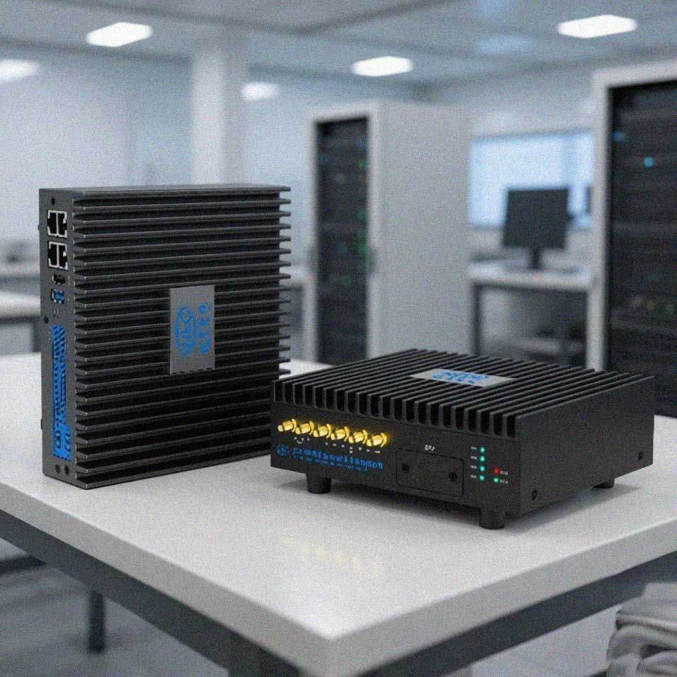
Overview
Edge computing gateway PCB design is the core link that determines the operating performance, reliability and deployment adaptability of edge computing gateway hardware. As the key connection node between end-side equipment and cloud platforms, edge computing gateways need to simultaneously undertake high-speed data collection, local real-time computing, 5G/ethernet data transmission, and multi-protocol conversion functions, and are often deployed in harsh industrial sites with large temperature differences, strong vibration, and complex electromagnetic interference. Poor PCB design will lead to problems such as signal attenuation, crosstalk between 5G RF and control signals, impedance mismatch, heat dissipation failure, and EMC non-compliance, which will directly increase data transmission delay, reduce computing accuracy, and even cause equipment downtime in severe cases. Professional edge computing gateway PCB design services cover the full process from schematic design, stack planning, component layout, high-speed routing optimization to testing and verification, fully addressing the core pain points of edge gateway hardware development, meeting the low-latency, high-stability, and ruggedness requirements of edge deployment scenarios, and adapting to multiple core processing platforms such as ARM, DSP, FPGA, and GPU.
Technical Capabilities
- Multi-Platform Hardware Compatibility: Supports design for ARM, DSP, FPGA, GPU core processing platforms, including high-performance 8-core edge processing chips, adapts to different computing power requirements from 4TOPS to 32TOPS, matches 5G module, Gigabit Ethernet, RS485, CAN bus, DI/DO and other industrial interface layout and signal isolation requirements, supports flexible expansion of peripheral modules according to scenario needs.
- High-Speed Signal Integrity Optimization: Supports high-speed I/O transmission up to 750Gbps, 10-layer and above stack design with up to 4 independent ground planes, effectively suppresses crosstalk between 5G RF signals, high-speed storage interfaces and low-speed control signals, achieves 100Ω/90Ω high-precision impedance control with error margin within ±5%, reduces signal reflection and attenuation, and ensures stable transmission of high-bandwidth data streams.
- Ruggedized Structural and Thermal Design: Provides targeted protective design for vibration, dust, humidity and wide temperature changes in industrial scenarios, supports buried copper block, buried component, embedded ceramic and other special process design to improve heat dissipation efficiency, avoids local overheating of high-computing-power chips under long-term full-load operation, ensures stable operation in -40℃ to +85℃ industrial temperature range, and meets IP30 to IP65 protection level requirements for different deployment environments.
- Full-Process Verification Support: Covers schematic review, stack planning, placement and routing optimization, DFM check, and post-production performance testing, including signal integrity test, EMC test, high and low temperature cycle test, vibration impact test, salt spray test and electrostatic protection test, to eliminate design defects before mass production and reduce the risk of post-launch product failure.
Quality Standards
- Industry Norm Compliance: All design processes comply with IPC-A-610, IPC-2221 and other international electronic assembly and PCB design standards, meet the electromagnetic compatibility requirements of EN 55032 and EN 61000 for industrial electronic equipment, and adapt to the access specifications of industrial Internet of Things platforms in different industries.
- Material Selection Control: Strictly select industrial-grade substrate materials with high TG, low CTE, and good dielectric constant stability, support high-frequency PTFE board materials for 5G RF signal transmission, avoid performance degradation caused by long-term operation in harsh environments, and extend the service life of finished products.
- Manufacturability Optimization: All designs go through DFM (Design for Manufacturing) and DFT (Design for Testing) checks, support micro-via as small as 0.06mm, line width/space as low as 2.0/2.0mil high-density routing requirements, ensure high yield in both 1-10 pieces prototype stage and 10k+ pieces mass production stage, and reduce manufacturing costs.
Applications
Edge computing gateway PCB design solutions are suitable for a wide range of industrial and smart city edge deployment scenarios, including but not limited to:
- Intelligent manufacturing factory equipment low-latency control and condition monitoring systems
- 5G connected industrial edge controller and industrial internet of things gateways
- Smart city edge computing nodes for video surveillance and environmental data collection
- Agricultural internet of things edge gateways for remote monitoring of planting and breeding sites
- Energy industry edge monitoring gateways for power grids, oil and gas pipelines
- Intelligent transportation edge gateways for road condition monitoring and vehicle data collection
- Smart retail edge gateways for offline store data collection and intelligent interaction
Key Advantages
- Customized Scheme Matching: Adjust PCB stack, routing rules, and protection design according to actual application scenarios, computing power requirements, and deployment environment, avoid over-design while meeting performance indicators, effectively reduce overall product costs by 15%-25% on average.
- Full-Lifecycle Service Coverage: Support end-to-end services from schematic design, PCB layout, prototype manufacturing, testing verification to mass production guidance, reduce cross-stage communication costs, shorten product R&D and launch cycle by 30% on average.
- Low-Latency Transmission Guarantee: Optimize the routing path of high-speed 5G signals and real-time control signals, minimize transmission path length, reduce end-to-end data transmission delay to below 10ms, meet the strict delay requirements of industrial real-time control scenarios such as robotic arm control and production line defect detection.
- Long-Term Reliability Assurance: All designs have passed 1000+ hours of accelerated aging test verification, the average failure-free operation time of finished products exceeds 50,000 hours, adapting to long-term uninterrupted operation requirements of industrial sites with high requirements for equipment stability.
Contact Information
If you have edge computing gateway PCB design requirements, whether for prototype verification, small-batch trial production or large-scale mass production, you can contact our technical team for consultation. We will provide you with free pre-design technical evaluation, targeted customized design solutions, and full-process technical support to help you quickly launch high-reliability edge computing gateway products that meet market demand.