Overview
Current transformer PCB design is a core technical link that directly determines the measurement accuracy, insulation safety, and long-term operation stability of current sensing equipment. Current transformers are responsible for converting high-voltage, high-current AC signals into low-voltage, low-current measurable signals while achieving electrical isolation between high-voltage loops and low-voltage control systems, and are widely used in power transmission, industrial control, and new energy scenarios. Poor design can easily lead to problems such as increased measurement error, insufficient insulation withstand voltage, eddy current loss, and signal crosstalk, which may cause equipment failure, misoperation of protection systems, and even safety accidents in severe cases. Professional current transformer PCB design services cover the entire process from schematic design, stack architecture planning, placement and routing optimization, simulation verification, to prototype performance testing, which can effectively solve core industry pain points, meet the application requirements of various complex scenarios, and ensure that products meet relevant international industry standards.
Technical Capabilities
- Insulation and Isolation Optimization: Supports multi-layer stack designs with dedicated isolation layers, meeting IEC 61800 creepage and clearance requirements for high-voltage scenarios up to 10kV. Designs integrate buried insulation materials and targeted copper thickness adjustments to eliminate cross-talk between high-voltage power loops and low-voltage sensing circuits, ensuring measurement error below 0.2% for rated current sampling.
- High-Precision Impedance Matching: Achieves ±5% impedance control accuracy for sensing signal paths, perfectly adapting to low-power analog signal transmission requirements of current transformer sensing units, reducing signal attenuation and harmonic distortion. Supports up to 0.5 pitch component placement for high-density multi-channel sensing array designs.
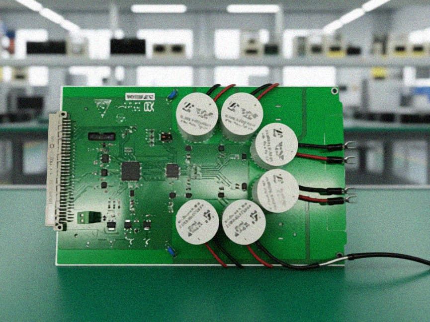
- Heavy Copper Construction Support: Supports 2-12 oz heavy copper PCB manufacturing for high-current primary loop designs, with optimized routing curvature and copper pour configurations to reduce eddy current loss and thermal accumulation, adapting to long-term operation under 100A+ continuous current loads without deformation or performance degradation.
- Special Material and Structure Adaptation: Supports a wide range of substrate materials including high-frequency laminates, ceramic substrates, and high-temperature resistant FR-4, as well as specialized structures such as buried copper blocks, buried resistance/capacitance boards, and semi-flexible boards, adapting to extreme operating conditions including high humidity, high vibration, and wide temperature ranges.
- High-Density Placement and Routing: Supports minimum 01005 (0.3mm0.2mm) component packaging placement, with design rules requiring ≥3mm clearance between surface components, mark points, and board edges to ensure welding reliability and test accessibility. Supports maximum board sizes up to 600mm450mm for integrated multi-channel current transformer array designs for distribution networks.
- Simulation-Driven Design Verification: Integrates electromagnetic field simulation, thermal simulation, and signal integrity simulation at the design stage, predicting potential problems such as eddy current heating, partial discharge, and signal interference in advance, reducing the number of prototype iterations and shortening the overall development cycle.
Quality Standards
- Electrical Performance Testing Standards: All designs undergo mandatory signal integrity testing, insulation withstand voltage testing, and insertion loss testing before mass production, ensuring compliance with IEC 60044-8 current transformer performance standards, with partial discharge levels below 10pC under rated voltage, and insulation resistance higher than 100MΩ at room temperature.
- Environmental Reliability Verification: Designs are validated for stable operation across a -40℃ to +125℃ industrial temperature range, passing 1000-hour high-temperature aging, 96-hour salt spray corrosion, and 10-2000Hz mechanical vibration testing to meet IP65 and higher protection level requirements for outdoor and industrial site deployment.
- Manufacturability Verification Standards: All design outputs undergo strict DFM (Design for Manufacturing) checks, including solder paste printing feasibility, reflow process compatibility, and X-Ray inspection alignment requirements, ensuring manufacturing yield above 98% for mass production runs, and less than 0.1% failure rate within the product warranty period.
- Material and Process Compliance: All selected materials and processes comply with RoHS, REACH, and halogen-free environmental requirements, adapting to global market access standards for electronic products.
Applications
Current transformer PCB design solutions can be widely applied to the following core scenarios:
- Power Grid Energy Metering Systems: Applied to high-voltage distribution network metering units, low-voltage smart meter sensing modules, and substation current monitoring systems, ensuring measurement accuracy meets 0.2S level commercial metering requirements.
- Industrial Motor Control Systems: Used in variable frequency drive current sensing modules, servo motor overcurrent protection units, and industrial robot power monitoring circuits, supporting fast response times below 1µs for overcurrent protection triggers to avoid equipment damage.
- New Energy Power Generation Systems: Adapted to photovoltaic inverter current monitoring units, wind turbine converter control modules, and energy storage system BMS current sensing arrays, adapting to high-frequency switching operation scenarios up to 100kHz.
- Electric Vehicle Charging Infrastructure: Applied to DC fast charging pile current measurement modules, on-board charger current monitoring units, and battery management system high-voltage sensing circuits, meeting 1000V+ high-voltage isolation requirements for new energy vehicle systems.
- Power Quality Monitoring Equipment: Used in harmonic analyzers, power quality recorders, and reactive power compensation device sensing modules, supporting accurate sampling of 0-50th harmonic current signals for grid operation analysis.
- Rail Transit Power Systems: Applied to subway traction power supply monitoring units, high-speed rail auxiliary power system current sensing modules, meeting the high anti-vibration and high reliability requirements of rail transit operation scenarios.
Key Advantages
- Full-Cycle Design Support: Covers end-to-end services from schematic optimization, stack planning, placement and routing adjustment, simulation verification, to prototype testing, adapting to requirements from proof-of-concept prototyping to large-scale mass production of 100k+ units.
- Customized Solution Matching: Provides targeted design adjustments based on application scenarios, including waterproof, anti-vibration, and explosion-proof structure optimization for special operating environments, reducing overall product development cycles by 30% on average compared to general design solutions.
- Cost-Optimized Design Logic: Balances performance requirements and manufacturing costs by selecting appropriate materials and process routes, avoiding over-design while ensuring product reliability, reducing overall product BOM costs by up to 15% without reducing performance indicators.
- Standardized Design Process: Follows a unified standardized design process, with clear output specifications for each link, reducing design errors caused by human factors, and ensuring consistency of product performance across different production batches.
Contact Information
If you have current transformer PCB design requirements, including custom specification adjustments, technical consultation, or design feasibility evaluation, please reach out to our technical support team. We will provide you with a targeted design plan and free pre-project technical assessment service within 2 working days, to help you achieve efficient landing of product development and mass production.