Overview
EMI/EMC PCB design is a core prerequisite for ensuring the stable operation and regulatory compliance of modern electronic hardware, especially as high-frequency, high-speed, and high-density circuit designs become increasingly mainstream. Uncontrolled electromagnetic interference (EMI) can lead to signal distortion, data transmission errors, functional failure of adjacent devices, and failure to pass mandatory regional regulatory certifications, directly extending product time-to-market and increasing development costs.
Professional EMI/EMC PCB design addresses these risks across the entire product development cycle, from initial schematic planning and stackup design to prototype testing and rectification, targeting core EMC challenges including radiated emissions, conducted interference, electrostatic discharge (ESD), and electromagnetic susceptibility. The design process balances performance, manufacturing feasibility, and compliance requirements to ensure products meet specified EMC grade standards for their target application scenarios.
Technical Capabilities
- Full-Cycle EMC Diagnosis and Analysis: End-to-end EMC risk assessment covering schematic review, stackup simulation, layout pre-verification, and prototype testing, to identify root causes of potential interference including unfiltered high-frequency signal outputs, inadequate ground plane isolation, and crosstalk between sensitive traces. Deliver detailed analysis reports with quantifiable interference indicators and targeted improvement suggestions.
- Component and Structural Optimization: Adjust component selection, single-board structure, and layer stackup configuration to minimize inherent interference sources, such as replacing low-grade filtering components with high-suppression equivalents, planning dedicated shielding layers for high-power circuits, and optimizing the physical structure of the board to reduce electromagnetic radiation leakage. All adjustments are made without compromising core product functional performance.
- Layout and Routing Adjustment for EMC Compliance: Optimize the placement of high-speed, high-power, and sensitive components to isolate interference sources from susceptible circuits, plan independent ground planes for different functional modules to reduce common impedance coupling, implement length matching and impedance control for high-speed differential signal traces, and avoid routing sensitive traces across split ground planes. These adjustments ensure the final design meets the required EMC grade standards for certification.
- Prototype Debugging and Rectification Support: Provide targeted rectification solutions for EMC test failures of existing prototypes, including adding filtering circuits, shielding structures, and surge protection components, adjusting trace routing or layer stackup as needed, and supporting repeated verification testing until the design passes all required EMC certification tests.
- Multi-Software and Revision Support: Compatibility with all mainstream PCB design software versions, supporting both new product design and revision of existing PCB files to upgrade EMC performance, eliminating the need for full redesign to reduce development costs. Services also include custom schematic library and component package library development to ensure design consistency and accuracy.
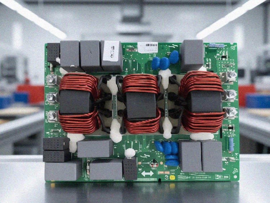
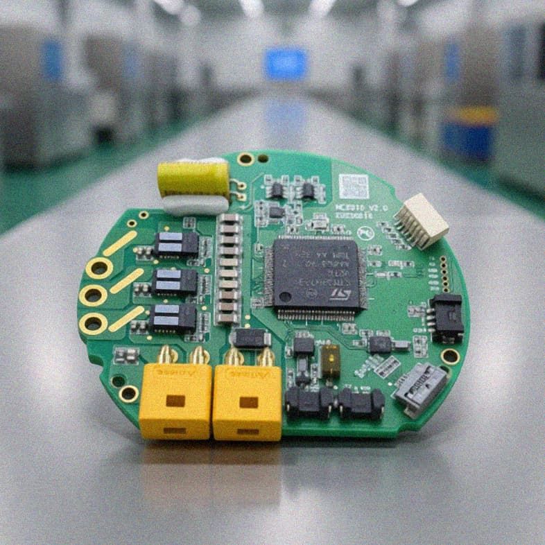
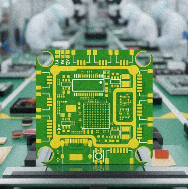
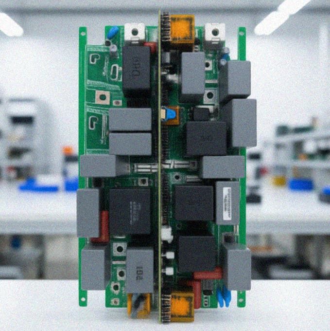
- Wide Range of Board Type Adaptation: Support EMI/EMC design for all common PCB categories, including single/double-sided boards, multilayer boards, HDI boards, rigid-flex boards, high-frequency boards, high-speed backplanes, buried resistance/capacitance boards, metal core boards, and IC substrate boards, adapting to the unique EMC requirements of different product types.
Quality Standards
All EMI/EMC PCB design processes follow globally recognized regulatory and industry standards, with mandatory verification checkpoints at each design phase to ensure compliance and performance consistency.
- Designs align with core EMC standard systems including CISPR, FCC Part 15, CE EN 55032, IEC 61000 series, and industry-specific standards for automotive, medical, and industrial applications, to ensure products pass regulatory certification in target sales regions.
- Pre-design simulation and post-design verification are mandatory for all projects, including signal integrity simulation, electromagnetic field simulation, and ESD susceptibility simulation, to identify potential risks before prototype production, reducing the number of design iterations and shortening development cycles.
- Material selection and manufacturing process specifications comply with RoHS, REACH, and other environmental protection requirements, with clear parameters for operating temperature range, vibration resistance, and humidity tolerance to adapt to harsh application environments.
- Impedance control accuracy meets industry-leading levels, with error margins controlled within ±5% for high-speed signal traces, ensuring stable signal transmission while minimizing unintended electromagnetic radiation.
Applications
EMI/EMC PCB design solutions are applicable to a wide range of electronic hardware scenarios with strict compliance and operational stability requirements, including but not limited to:
- Industrial control equipment: Ensure stable operation in factory floor environments with high levels of electromagnetic interference, complying with industrial EMC standards to avoid functional failure that causes production downtime.
- Medical electronic devices: Meet strict EMC requirements for patient safety, preventing interference between medical devices and ensuring the accuracy of diagnostic and therapeutic equipment.
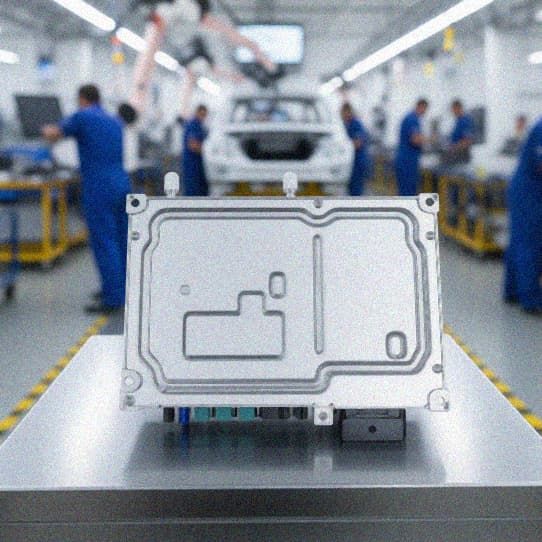
- Automotive electronics: Comply with automotive EMC standards such as ISO 11452, supporting design for in-vehicle infotainment systems, autonomous driving domain controllers, sensor modules, and powertrain control units.
- Communication infrastructure: Design for 5G base stations, core network equipment, and edge communication nodes, suppressing electromagnetic interference between high-power transmission modules and sensitive receiving circuits to ensure communication stability.
- Consumer electronics: Meet FCC, CE and other regional regulatory requirements for smart home devices, wearable electronics, and consumer computing products, avoiding interference with other household electronic devices.
- Aerospace and defense systems: Adapt to harsh electromagnetic environments in aerospace and military applications, with high EMC protection levels to resist external interference and ensure information security.
- IoT edge devices: Optimize EMC performance for low-power, high-density edge computing and sensing devices, ensuring stable data transmission in dense deployment scenarios.
Key Advantages
- Compliance-First Design Logic: All design processes prioritize EMC compliance requirements based on the product's target industry and sales region, avoiding costly post-production redesigns caused by non-compliance, and shortening overall product time-to-market by 20-30% compared to non-specialized design processes.
- Cost-Effective Performance Balance: Design solutions balance EMC performance and manufacturing cost, avoiding over-design such as unnecessary additional shielding layers or high-cost components that increase production expenses, while ensuring all mandatory EMC and functional performance indicators are fully met.
- Cross-Domain Technical Experience: Proven design experience across all major industry verticals, with deep understanding of industry-specific EMC requirements and common interference challenges, enabling targeted design optimization for different application scenarios.
- End-to-End Service Coverage: Support covers the entire product development cycle from initial schematic design, component library development, PCB layout, prototype manufacturing guidance, to EMC test debugging and mass production optimization, reducing cross-team communication friction and ensuring design feasibility for mass production.
Contact Information
If you have EMI/EMC PCB design requirements, whether for new product development, existing PCB file revision, or EMC test failure rectification, you can reach out to the technical team for support. We provide customized design solutions tailored to your specific project requirements, as well as free pre-project technical evaluation and professional consulting services to help you achieve EMC compliance and stable product operation.