International orders follow standard B2B payment terms agreed during quoting, typically bank transfer with deposit and balance stages for new customers and credit terms for established accounts.
View More >>
If your problem is still not resolved, you can search or consult our experts.
International orders follow standard B2B payment terms agreed during quoting, typically bank transfer with deposit and balance stages for new customers and credit terms for established accounts.
View More >>Engineering changes are managed through a formal change process: the change request is reviewed for impact on cost, lead time, and reliability, then implemented with version control and documentation.
View More >>Yes.
View More >>Evaluate five dimensions: technical capability (layer count, materials, impedance, special processes), certifications (ISO 9001, industry-specific like IATF 16949/ISO 13485/AS9100D), quality system (testing, failure analysis, traceability), responsiveness (engineering support, quoting speed, communication), and supply chain (component sourcing, capacity, no-MOQ flexibility).
View More >>HDI PCBs use laser-drilled microvias (down to 0.06 mm), via-in-pad, and sequential lamination to achieve higher wiring density in less area, while standard PCBs use through-hole vias on FR4 with larger feature sizes.
View More >>Switch from standard FR4 to low-loss materials when channel rates exceed roughly 10-25G per lane, when link length is long, or when insertion loss budget is tight (224G designs, backplanes, optical modules).
View More >>ENIG is best for fine-pitch SMD, BGA, and long shelf life; HASL is cost-effective for through-hole and standard SMD but less suited to fine pitch; OSP is low cost and flat but offers limited shelf life and weaker for repeated handling.
View More >>Moving to production, design files should be optimized for yield: wider tolerances where acceptable, panelization for efficiency, standard materials with shorter lead times, and DFM-verified stack-ups.
View More >>Impedance mismatches cause signal reflection, ringing, and higher bit-error rates as data rates rise.
View More >>PCB cost is driven by layer count, board area, material grade, minimum feature size, hole density, surface finish, special processes, quantity, and delivery speed.
View More >>Common PCB defects come from design (spacing, impedance, thermal issues), materials (warpage, moisture), and process (plating voids, solder defects, misregistration).
View More >>For 112G/224G channels, choose ultra-low-loss laminates with stable Dk/Df over frequency and temperature, such as Panasonic M6/M7N/M8N and TUC TU933+/TU943N families, paired with low-profile copper.
View More >>
Founded in 1997 and headquartered in Shenzhen, KINGBROTHER specializes in electronic interconnection technologies and hardware innovation. We focus on electronic product R&D, AI hardware solutions, engineering services, integrated design and manufacturing, and supply chain capabilities to deliver comprehensive PCB manufacturing, IPD (Integrated Product Development), and EMS services.
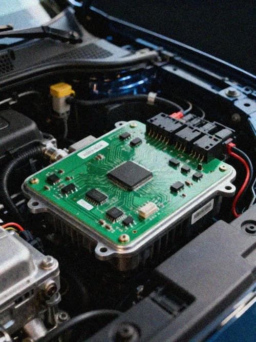
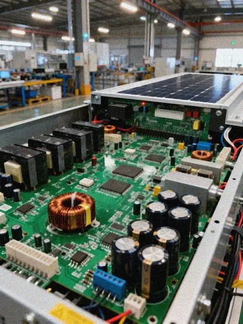
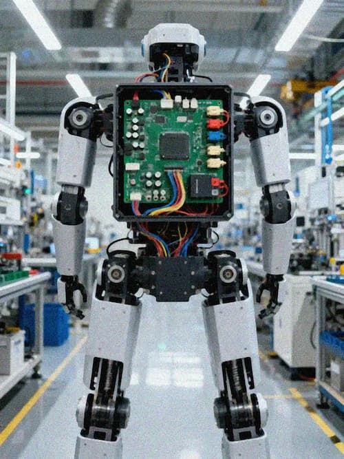
We are committed to becoming a world-class AI hardware solutions and manufacturing service provider, offering one-stop solutions for AI robots, industrial control, medical devices, new energy, and automotive electronics, helping our customers accelerate innovation and bring products to market faster.
We adhere to systematic design as our foundation, offering hardware, software, and industrial design services. With 6 self-owned design centers and a knowledge base including 3.27 million certified materials and 2,368 DFI rules, we significantly reduce design iterations by 60-80% and increase customer project success rates by 35%.
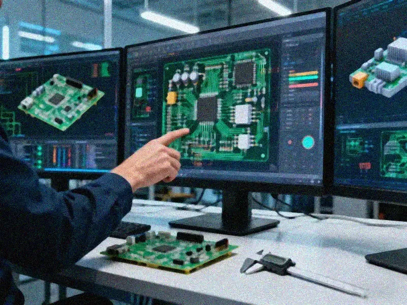
We have built an integrated technology chain from IC design IPD and PCB to integrated product manufacturing IPI. With 300+ technical solutions and over 2,500,000 product models and project verifications, we achieve closed-loop collaboration and optimization throughout the hardware innovation process.
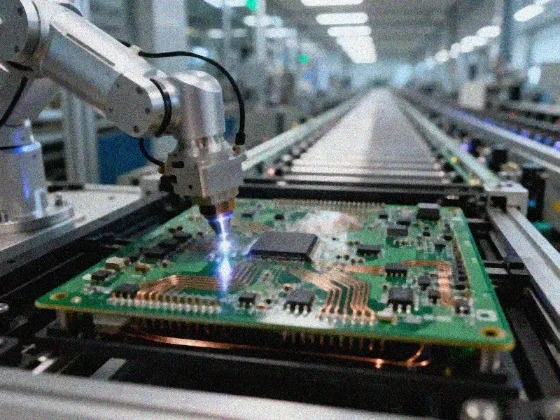
Through strict QIS quality management systems and full-chain engineering empowerment via DF8, failure analysis, and process control, we eliminate 90% of pad defects and 70% of assembly risks, ensuring product safety for our customers.
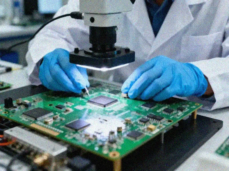
Leveraging 5 IPI smart manufacturing bases and a cloud alliance of over 100 factories, we have established a flexible production system for small-batch, multi-batch needs. Our mature global supply chain ensures quick response and delivery, especially in component procurement.
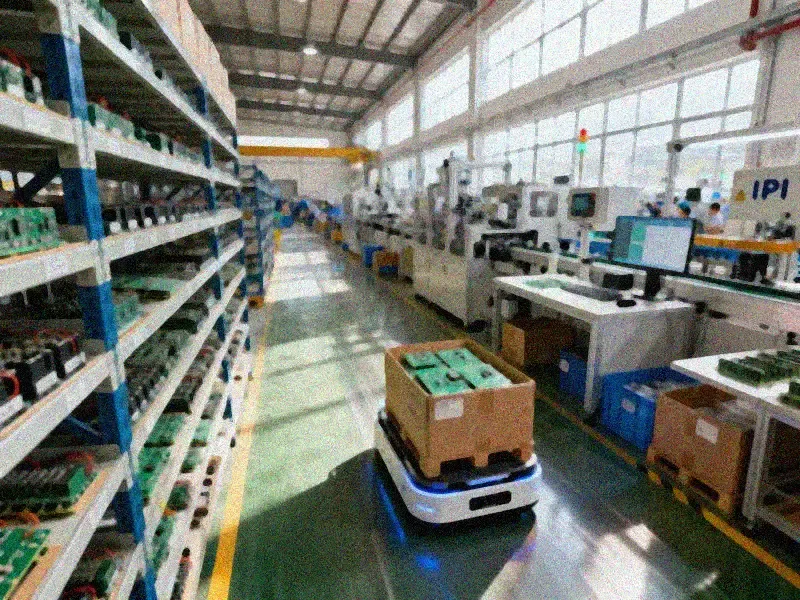



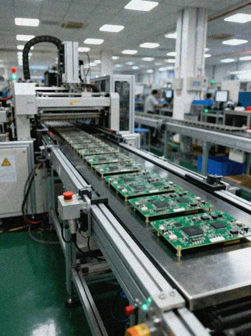
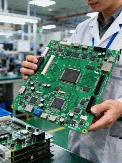
With 29 years of expertise in high-end and specialty PCBs, we deliver reliable and flexible manufacturing solutions. We offer prototyping, quick-turn, and small-to-medium volume PCBs, including multilayer, HDI, high-copper, and rigid-flex boards, backed by a one-stop PCB service that empowers clients across industries, from AI hardware to cutting-edge electronics, to accelerate product innovation and bring ideas to market faster.
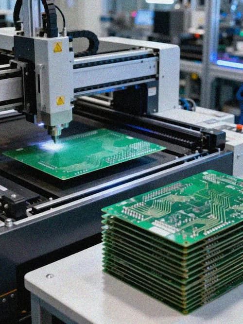
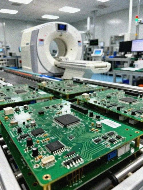
Reliable AI hardware solutions with full-lifecycle supply chain support. We provide highly reliable electronic manufacturing services. Our integrated PCBA, BOM management, NPI engineering and advanced failure analysis to guarantee reliable performance at every stage.
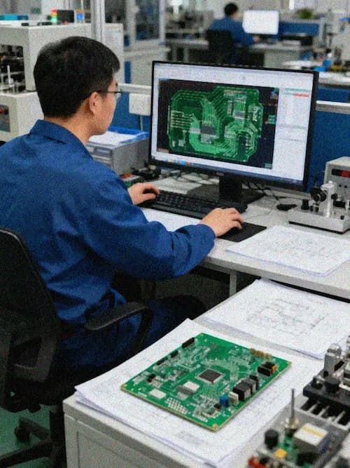
We focus on independent design house (IDH) and CAD design, providing AI hardware solutions and covering services such as hardware design, software design, industrial design, and EDA development.
100% Complete & Professional Solutions: From Design to Manufacturing.